Touch panel

a touch panel and touch technology, applied in the field of touch panel, can solve the problems of difficult to detect two or more contacts (multiple touches) concurrently, difficult to provide a large screen in view of responsiveness, etc., and achieve the effect of easy manufacturing and large tolerance for laying errors

Active Publication Date: 2013-09-19
FUJIFILM CORP
View PDF12 Cites 75 Cited by
  • Summary
  • Abstract
  • Description
  • Claims
  • Application Information

AI Technical Summary

Benefits of technology

[0015]According to the touch panel of the present invention, due to large tolerance for errors in laying the first electrode and the second electrode on each other or for shape errors in the conducting wires, it is possible to obtain a novel conducting wire pattern whose grid-like shape does not look incompatible even when the first electrode and the second electrode are misaligned to some extent or there is a variety among the shapes of the conducting wires. That is, it is possible to provide a capacitive or resistive touch panel which can be manufactured easily using thin wires such as metal thin wires.

Problems solved by technology

It is, however, difficult to provide a large screen in view of responsiveness due to the high resistance value of ITO.
It is therefore difficult to detect two or more contacts (multiple touches) concurrently.

Method used


Image

  • Touch panel
  • Touch panel
  • Touch panel

Examples


Embodiment Construction

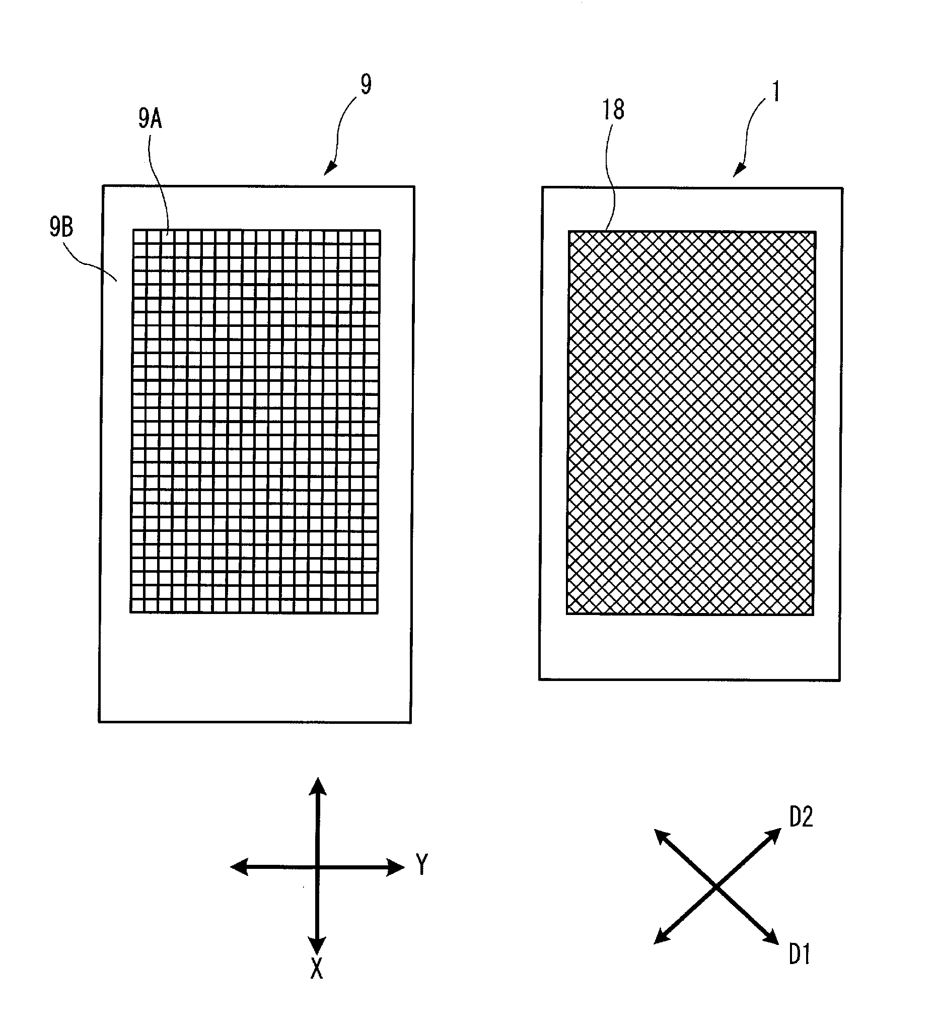
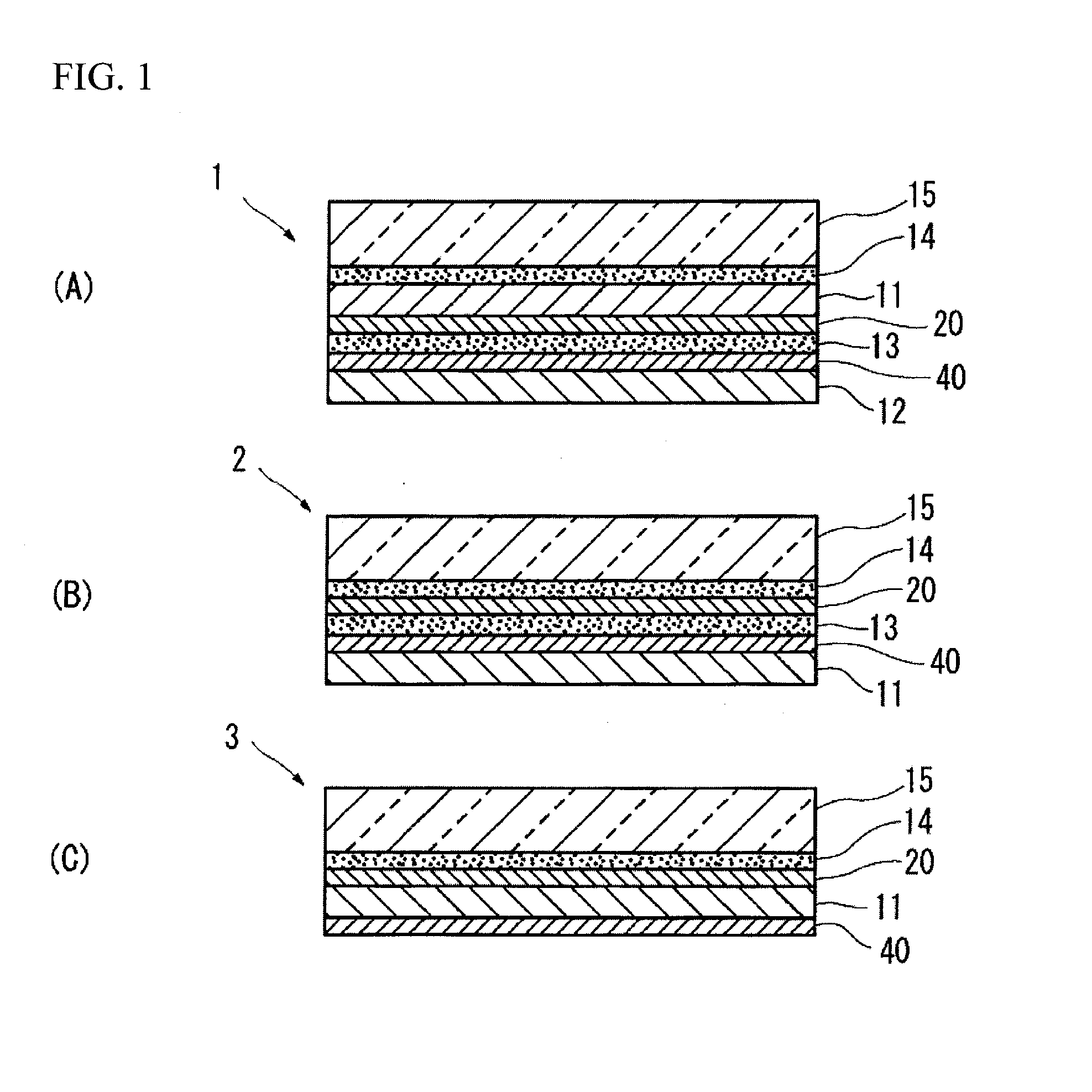
[0052]Embodiments of capacitive touch panels for explaining a mode for carrying out the invention will be described with reference to FIGS. 1 to 9.

[0053]The sign “−” used in this specification implies that numeral values indicated before and after the sign are included as a lower limit and an upper limit.

[0054](A) to (C) of FIG. 1 schematically show sectional views of embodiments of projected capacitive touch panels according to the present invention respectively. Each of the touch panels 1 to 3 is a stack of a plurality of layers, including an upper electrode 20 serving as a first electrode disposed on the side to be touched by a fingertip, and a lower electrode 40 laid on the upper electrode 20 and serving as a second electrode disposed on the side of a display 9 (FIG. 9) as an image display unit. The configurations of (A) to (C) of FIG. 1 are different from one another in the positions where the upper electrode 20 and the lower electrode 40 are arranged in the stack. Incidentally...


PUM


Abstract

A touch panel includes: a first electrode in which second-direction parallel bands having a plurality of conducting wires disposed to extend in parallel with one another and along a second direction intersecting with a first direction are formed repeatedly in the first direction with interposition of first-direction gaps in the first direction, and first-direction cross bands having conducting wires disposed to extend in the first direction and intersect with the second-direction parallel bands are formed repeatedly in the second direction; and a second electrode in which first-direction parallel bands are formed as defined herein, and second-direction cross bands are formed as defined herein, and the first electrode and the second electrode are laid on each other so that the second-direction cross bands correspond to positions of the first-direction gaps and the first-direction cross bands correspond to positions of the second-direction gaps.

Description

[0001]This is a continuation of International Application No. PCT / JP2011 / 075118 filed on Oct. 31, 2011, and claims priority from Japanese Patent Application No. 2010-249208 filed on Nov. 5, 2010, the entire disclosures of which are incorporated herein by reference.TECHNICAL FIELD[0002]The present invention relates to a touch panel (touch screen). Particularly, the present invention relates to a capacitive touch panel or a resistive touch panel in which electrode arrays are formed out of a thin wire pattern in each of two different layers so that multiple touches can be detected.BACKGROUND ART[0003]Analog resistive technology in which electric conduction is detected in a touch position between two conductive layers (electrode layers) disposed to be opposed to each other through a dot spacer has been often used in touch panels (for example, Patent Literature 1). In recent years, capacitive touch panels in which a touch position of a fingertip is detected using a change of electrostati...

Claims


Application Information

Patent Timeline
Patent Type & Authority Applications(United States)
IPC IPC(8): H05K7/02
CPCG06F3/041G06F2203/04104H05K7/02G06F2203/04103G06F3/0412G06F3/0445G06F3/045G06F2203/04112
Inventor OHTANI, SUMIOKURIKI, TADASHI
Owner FUJIFILM CORP
Why Eureka
Try Eureka