Semiconductor chip and stacked semiconductor package having the same

a technology of semiconductor package and semiconductor chip, which is applied in the direction of semiconductor device, semiconductor/solid-state device details, electrical apparatus, etc., can solve the problems of poor connection and serious and achieve the effect of improving alignment precision and preventing the occurrence of poor connection

Inactive Publication Date: 2013-11-07
SK HYNIX INC
View PDF2 Cites 0 Cited by
  • Summary
  • Abstract
  • Description
  • Claims
  • Application Information

AI Technical Summary

Benefits of technology

[0009]An embodiment is directed to a semiconductor chip which can provide an improved alignment precision when stacking semiconductor chips, thereby being suitable for preventing the occurrence of a poor connection between semiconductor chips.

Problems solved by technology

In the stacked semiconductor package using such through electrodes, if a misalignment occurs between stacked semiconductor chips, the positions of the through electrodes of an upwardly positioned semiconductor chip and the through electrodes of a downwardly positioned semiconductor chip are not aligned with each other, by which a poor connection occurs.
Further, the occurrence of a poor connection becomes serious as the pitch of the through electrodes decreases by an influence of high integration.

Method used


Image

  • Semiconductor chip and stacked semiconductor package having the same
  • Semiconductor chip and stacked semiconductor package having the same
  • Semiconductor chip and stacked semiconductor package having the same

Examples


Embodiment Construction

[0041]Hereafter, embodiments will be described in detail with reference to the accompanying drawings.

[0042]It is to be understood herein that the drawings are not necessarily to scale and in some instances proportions may have been exaggerated in order to more clearly depict certain features of the embodiments. The same reference numerals or the same reference designators may denote the same elements throughout the specification.

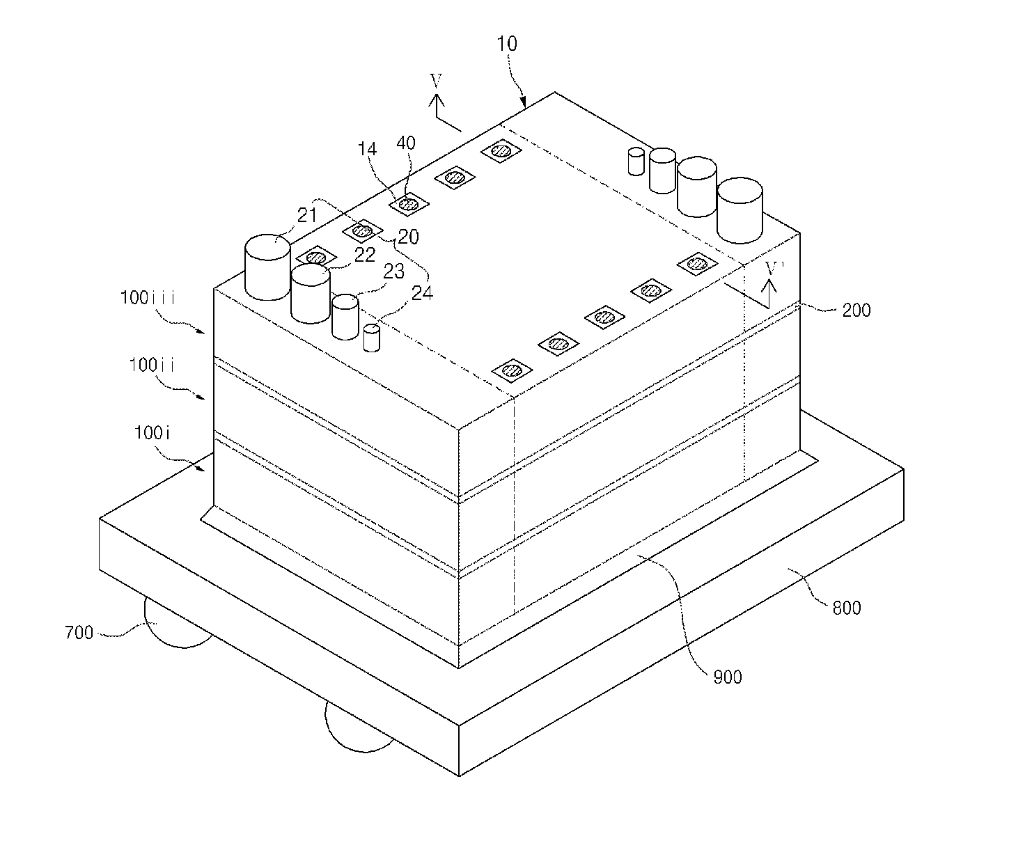
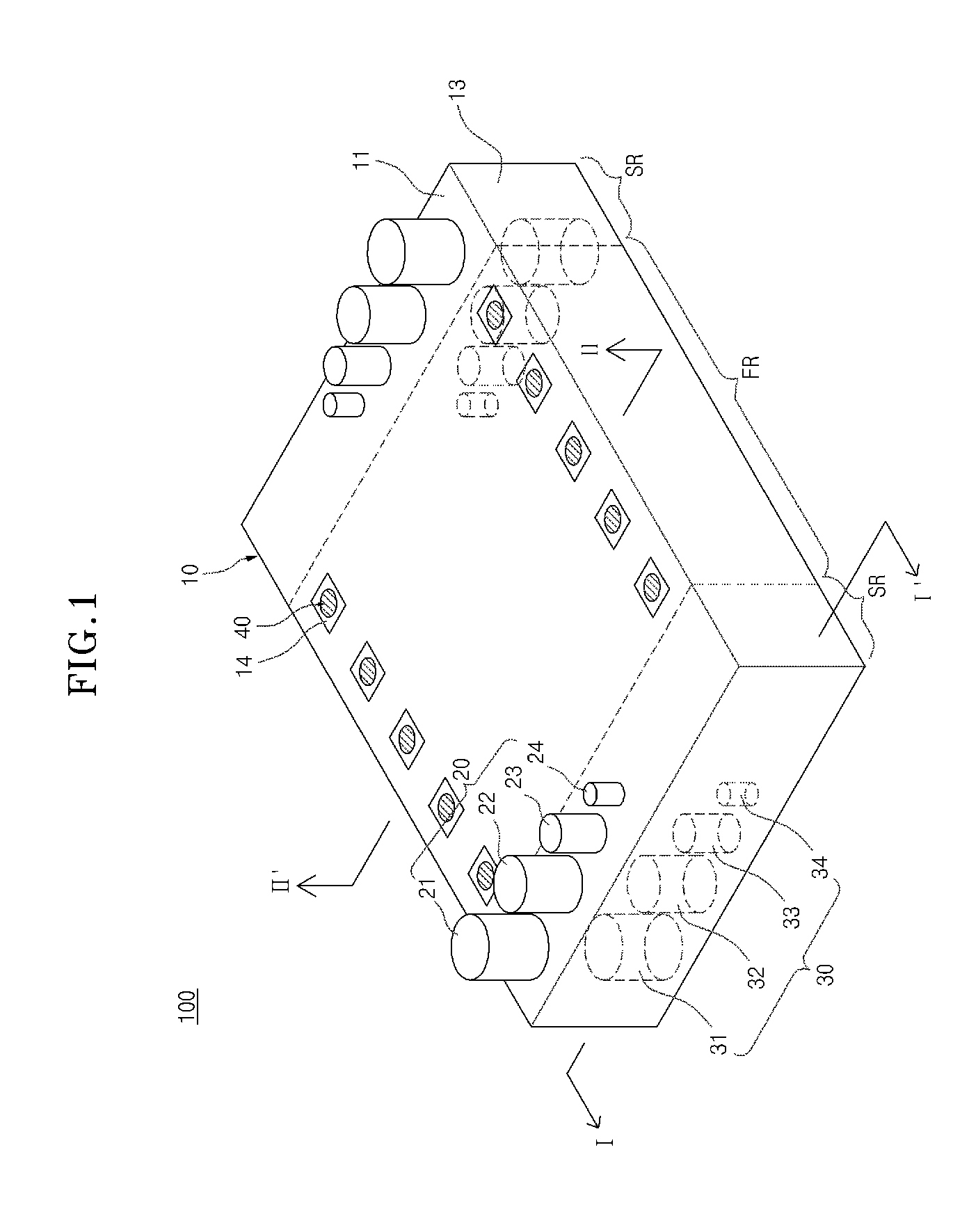
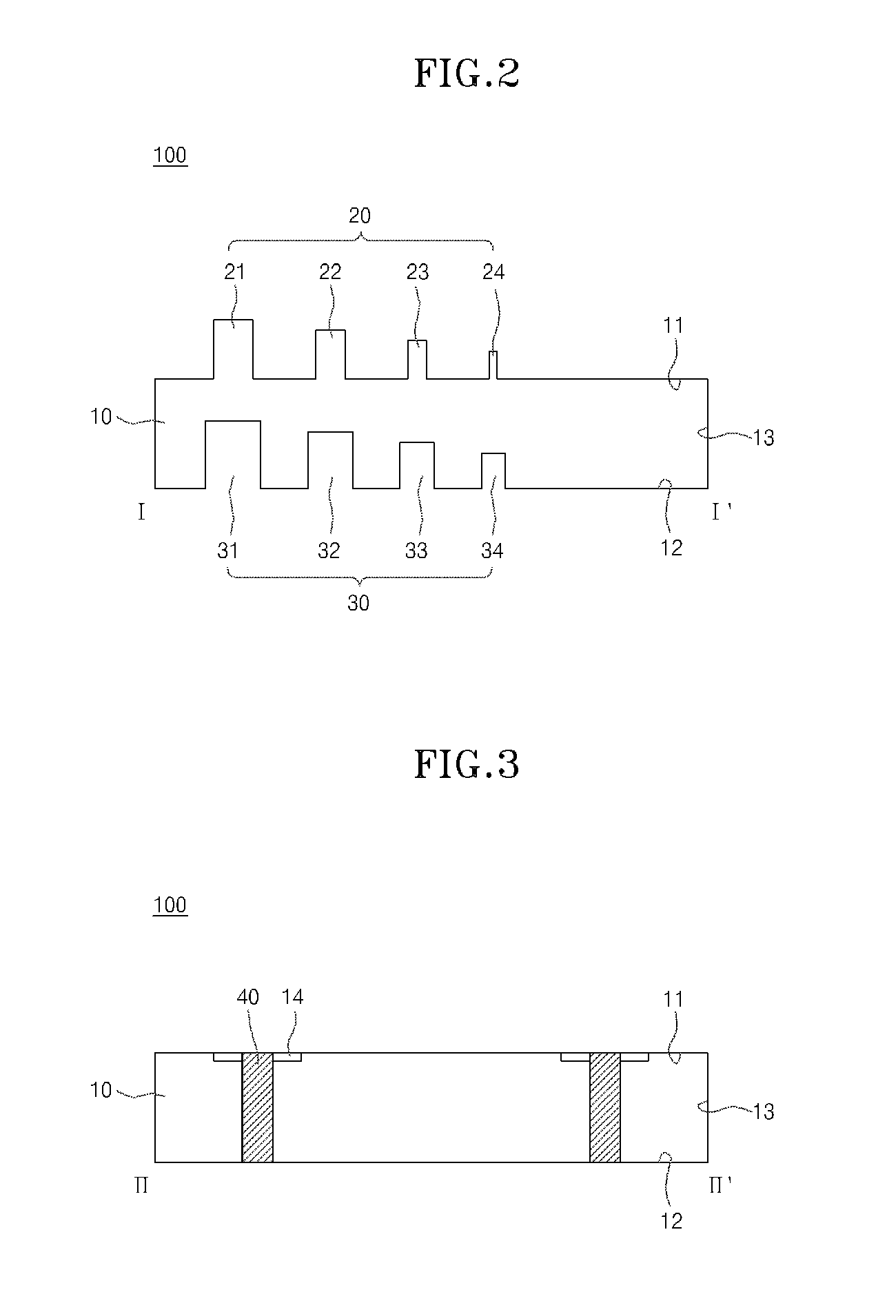
[0043]FIG. 1 is a perspective view illustrating a semiconductor chip in accordance with an embodiment of the present invention, FIG. 2 is a cross-sectional view taken along the line I-I′ of FIG. 1, and FIG. 3 is a cross-sectional view taken along the line II-II′ of FIG. 1.

[0044]Referring to FIGS. 1 to 3, a semiconductor chip 100 in accordance with an embodiment may include a substrate 10, a plurality of alignment bumps 20, and a plurality of alignment grooves 30. Besides, the semiconductor chip 100 further may include through electrodes 40.

[0045]The substrat...


PUM


Abstract

A semiconductor chip includes a substrate having one surface and an other surface which substantially faces away from the one surface; at least two alignment bumps formed on the one surface of the substrate and having different diameters; and at least two alignment grooves defined on the other surface of the substrate and having different diameters.

Description

CROSS-REFERENCE TO RELATED APPLICATIONS[0001]The present application claims priority under 35 U.S.C. 119(a) to Korean Patent Application Number 10-2012-0047062 filed in the Korean Intellectual Property Office on May 3, 2012, which is incorporated herein by reference in its entirety.BACKGROUND[0002]1. Field of the Invention[0003]The present invention generally relates to a semiconductor device, and more particularly, to a semiconductor chip which can provide an improved alignment precision when stacking semiconductor chips, thereby being suitable for preventing the occurrence of a poor connection between semiconductor chips, and a stacked semiconductor package having the same.[0004]2. Description of the Related Art[0005]Packaging technologies for a semiconductor device have been continuously developed according to demands toward miniaturization and high capacity, and recently, various technologies for a stacked semiconductor package capable of satisfying miniaturization, high capacit...

Claims


Application Information

Patent Timeline
Patent Type & Authority Applications(United States)
IPC IPC(8): H01L23/498
CPCH01L23/544H01L24/81H01L25/0657H01L25/50H01L2223/54426H01L2223/54473H01L2224/16145H01L2224/16225H01L2224/32145H01L2224/32225H01L2224/73204H01L2224/81141H01L2225/06513H01L2225/06517H01L2225/06541H01L2225/06565H01L2225/06593H01L2924/15311H01L2924/00012H01L2924/00H01L23/12H01L23/48H01L2225/06555
Inventor LEE, JIN HUI
Owner SK HYNIX INC
Why Eureka
Try Eureka