Exposure method for glass substrate of liquid crystal display

a liquid crystal display and glass substrate technology, applied in the direction of microlithography exposure apparatus, instruments, photomechanical treatment, etc., can solve the problems of inability to monitor the misalignment of the inability to measure the alignment accuracy information, so as to improve the production yield of lcd panels, enhance the alignment precision between the tft array substrate and the color filter substrate, and effectively monitor the alignment precision

Active Publication Date: 2015-09-15
TCL CHINA STAR OPTOELECTRONICS TECH CO LTD
View PDF1 Cites 0 Cited by
  • Summary
  • Abstract
  • Description
  • Claims
  • Application Information

AI Technical Summary

Benefits of technology

[0005]The present invention aims to solve the technical problems and provides an exposure method for a glass substrate of a liquid crystal display, which is able to enhance the alignment precision between the TFT array substrate and the color filter substrate and increase the production yield of LCD panels.
[0006]It is to reduce cost while improving the property of an array substrate.
[0035]In the embodiments of the present invention, by way of joint exposure on the large-size LCD glass substrate, and performing exposure with each the photo mask on a separate reference substrate and performing measurement of the alignment precision measure and check marks, deformation and deflection levels of the exposed pattern can be obtained. The parameter of exposure in each exposure region can be modified according to the measurement result so as to make the alignment precision of the final exposed pattern formed after the joint exposure on the glass substrate located within the specified range. Accordingly, the alignment precision in the stitching region between adjacent exposure regions can be effectively monitored, the alignment precision between the TFT array substrate and the color filter substrate can be enhanced, and the production yield of LCD panels can be increased.

Problems solved by technology

As such, no alignment precision information can be measured for each of the two exposed regions at the side of the stitching exposure region, so the pattern deflection and deformation level cannot be monitored herein.
Thus the TFT array substrate might misalign with the color filter substrate, and defects, e.g. light leakage problem, of the LCD might occur.

Method used


Image

  • Exposure method for glass substrate of liquid crystal display
  • Exposure method for glass substrate of liquid crystal display
  • Exposure method for glass substrate of liquid crystal display

Examples


Embodiment Construction

[0046]Hereinafter, detailed descriptions of preferred embodiments according to the invention are given with annexed drawings.

[0047]Referring to FIG. 4, which is a primitive flowchart of an exposure method for a glass substrate of a liquid crystal display provided according to an embodiment of the present invention. In this embodiment, the exposure method for a glass substrate of a liquid crystal display includes the following steps.

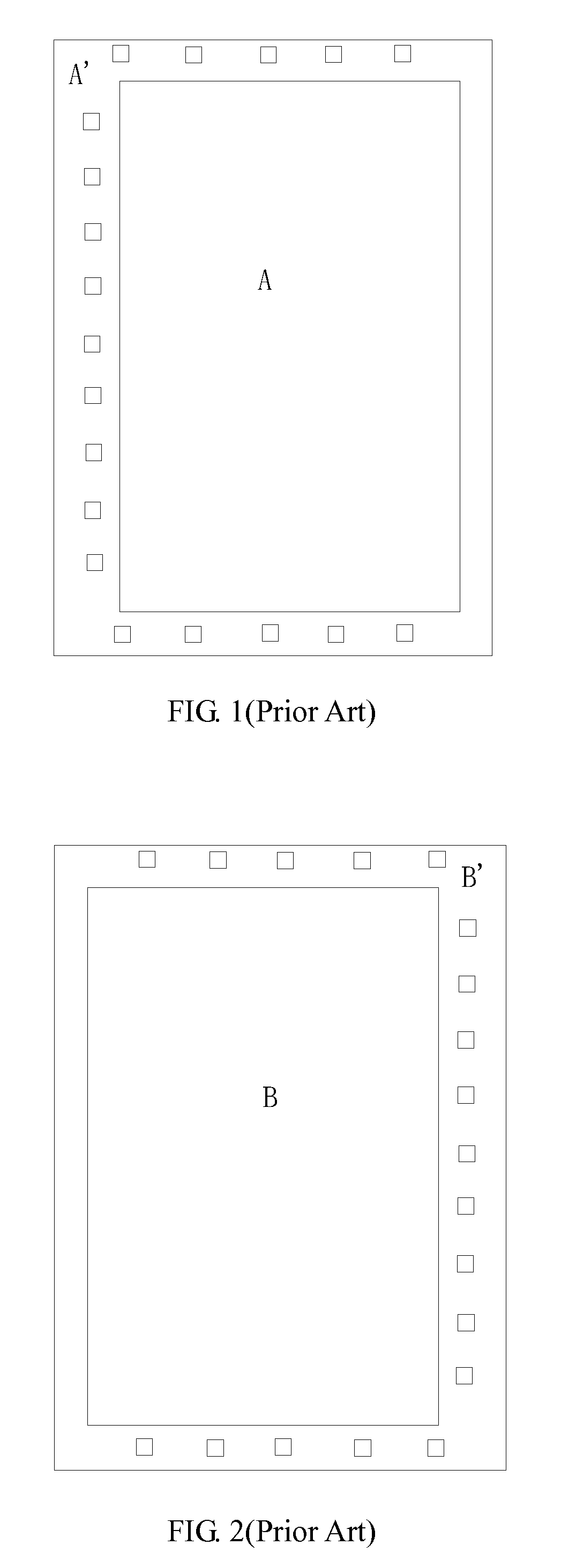
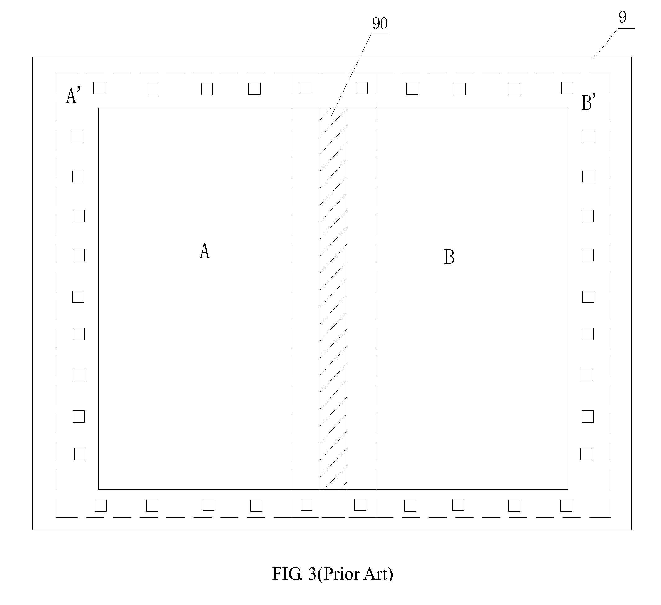
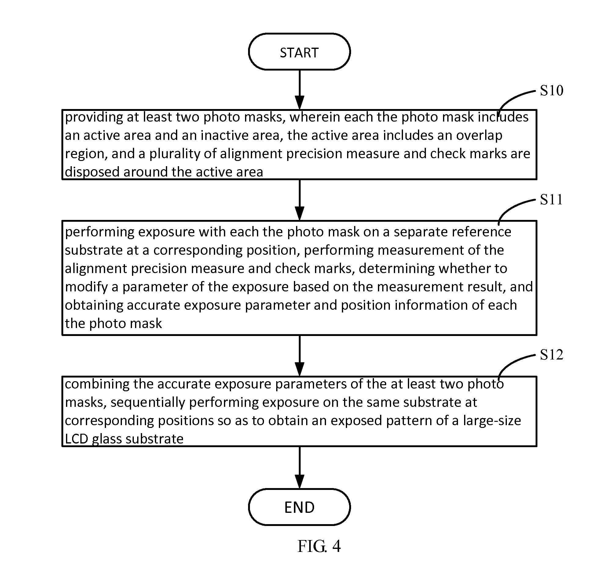
[0048]In Step S10, at least two photo masks are provided. Refer to FIG. 5 and FIG. 6 for the structure of the photo masks. In the structure, each the photo mask 1 includes an active area (Area A or Area B) and an inactive area (Area A′ or Area B′). An overlap region (Area A1 or Area B1) is included at a side of the active area. The overlap region is correspondingly disposed at the side of a stitching region of the glass substrate. Around the inactive area, alignment precision measurement and check marks, which are shown as small blocks in the figures, are...


PUM

PropertyMeasurementUnit
dimensionaaaaaaaaaa
sizeaaaaaaaaaa
structureaaaaaaaaaa

Abstract

An exposure method for an LCD glass substrate is revealed and includes: providing at least two photo masks, wherein each the photo mask includes active and inactive area with alignment-precision measurement-and-check marks disposed around the active area; performing exposure with each the photo mask on a separate reference substrate at a corresponding position, performing measurement of the alignment-precision measurement-and-check marks formed on the reference substrate, determining whether to modify a parameter of the exposure based on the measurement result, and obtaining accurate exposure parameter of each the photo mask; and combining the accurate exposure parameter of each the photo mask, using the combined exposure parameter to perform exposure sequentially with the at least two photo masks on the same substrate at corresponding positions, thereby obtaining an exposed pattern. Accordingly, the alignment precision between the TFT array and color filter substrates is enhanced and the LCD-panel production yield is increased.

Description

CROSS REFERENCE TO RELATED APPLICATIONS[0001]The present application claims priority to Chinese Patent Application No. 201310747958.2, filed Dec. 31, 2013, and entitled “EXPOSURE METHOD FOR GLASS SUBSTRATE OF LIQUID CRYSTAL DISPLAY”. The entire contents of the above-mentioned patent application are cited and incorporated herein for reference.FIELD OF THE INVENTION[0002]The present invention relates to a manufacturing technique of a thin film transistor liquid crystal display (TFT-LCD), and more particularly to an exposure method for a glass substrate of a liquid crystal display.BACKGROUND OF THE INVENTION[0003]With the rapid development of thin film transistor liquid crystal displays, the dimension of a liquid crystal display can be getting larger and larger. Consequently, it happens in an exposure process that the size of the pattern on a single large-size glass substrate is larger than that of a photo mask. Under this circumstance, it is necessary to device the pattern of the phot...

Claims


Application Information

Patent Timeline
Patent Type & Authority Patents(United States)
IPC IPC(8): G02F1/133G03F7/20G02F1/1333
CPCG03F7/2022G02F1/133308G03F7/70475G02F2001/133302G02F2001/133322G02F1/1333G02F1/133354G02F1/133302G02F1/133322
Inventor FU, YANFENG
Owner TCL CHINA STAR OPTOELECTRONICS TECH CO LTD
Why Eureka
Try Eureka