Light emitting device

a technology of light emitting diodes and diodes, which is applied in the direction of semiconductor devices, basic electric elements, electrical equipment, etc., can solve the problems of lowering the alignment precision between the light emitting diodes and the external circuit, and achieve the effect of better alignment precision

Active Publication Date: 2017-10-17
PLAYNITRIDE
View PDF8 Cites 2 Cited by
  • Summary
  • Abstract
  • Description
  • Claims
  • Application Information

AI Technical Summary

Benefits of technology

[0006]The invention provides a light emitting device having better alignment precision between micro light emitting chips and a substrate.
[0021]Based on the above, since the orthogonal projection area of each of the conductive bumps of the light emitting device of the invention on the substrate is greater than the orthogonal projection area of each of the micro light emitting chips on the substrate, namely, the orthogonal projection area of the conductive bumps is greater than the contact area between the micro light emitting chips and the conductive bumps. Therefore, there may be a larger alignment margin between the conductive bumps and the pads of the substrate, consequently aiding in increasing the alignment precision between the micro light emitting chips and the substrate.

Problems solved by technology

Wherein, a contact area of the conductive bumps or the solder with the light emitting diode chip is lesser than an area of the light emitting diode chip, therefore there is not an adequate alignment margin between the conductive bumps or the solder with the pads of the external circuit, consequently lowering the alignment precision between the light emitting diode chip and the external circuit.

Method used


Image

  • Light emitting device
  • Light emitting device
  • Light emitting device

Examples


Embodiment Construction

[0030]Reference will now be made in detail to the present preferred embodiments of the invention, examples of which are illustrated in the accompanying drawings. Wherever possible, the same reference numbers are used in the drawings and the description to refer to the same or like parts.

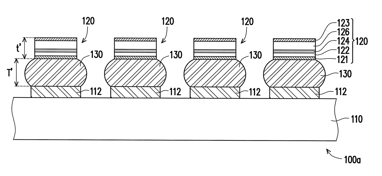
[0031]FIG. 1 is a cross-sectional schematic diagram illustrating a light emitting device according to an embodiment of the invention. Referring to FIG. 1, in the present embodiment, a light emitting device 100a includes a substrate 110, a plurality of micro light emitting chips 120 and a plurality of conductive bumps 130. The substrate 110 has a plurality of pads 112. The micro light emitting chips 120 are disposed on the substrate 110 in dispersion, wherein each of the micro light emitting chips 120 includes a P-type semiconductor layer 122, an active layer 124 and an N-type semiconductor layer 126. The conductive bumps 130 are disposed corresponding to the micro light emitting chips 120 and located...


PUM


Abstract

A light emitting device includes a substrate, a plurality of micro light emitting chips and a plurality of conductive bumps. The substrate has a plurality of pads. The micro light emitting chips are disposed on the substrate in dispersion. Each of the micro light emitting chips includes an N-type semiconductor layer, an active layer and a P-type semiconductor layer. The conductive bumps are disposed corresponding to the micro light emitting chips and located between the micro light emitting chips and the substrate. The micro light emitting chips are electrically connected to the pads of the substrate by the conductive bumps. An orthogonal projection area of each of the conductive bumps on the substrate is greater than an orthogonal projection area of each of the micro light emitting chips on the substrate.

Description

CROSS-REFERENCE TO RELATED APPLICATION[0001]This application claims the priority benefits of U.S. provisional application Ser. No. 62 / 081,503, filed on Nov. 18, 2014, U.S. provisional application Ser. No. 62 / 092,265, filed on Dec. 16, 2014 and Taiwan application serial no. 104134510, filed on Oct. 21, 2015. The entirety of each of the above-mentioned patent applications is hereby incorporated by reference herein and made a part of this specification.BACKGROUND OF THE INVENTION[0002]1. Field of the Invention[0003]The present invention relates to a semiconductor device, and relates particularly to a light emitting device.[0004]2. Description of Related Art[0005]Generally speaking, a light emitting diode chip may be electrically connected with an external circuit by a wire bonding or a flip-chip bonding method. In the flip-chip bonding connection method, the electrodes of the light emitting diode chip may be electrically connected with the pads on the external circuit by the conductive...

Claims


Application Information

Patent Timeline
Patent Type & Authority Patents(United States)
IPC IPC(8): H01L25/075H01L33/06H01L33/62H01L33/02H01L33/46
CPCH01L25/0753H01L33/62H01L2924/0002H01L2924/00H01L2224/95H01L2924/12041H01L24/83H01L24/95H01L24/29H01L24/05H01L2224/04026H01L2224/83805H01L2224/83203H01L2224/83825H01L2224/13144H01L2224/13111H01L2224/13109H01L2224/13116H01L2224/05599H01L2224/81409H01L2924/00012H01L2924/00014H01L2924/013H01L24/00
Inventor LAI, YU-HUNGLIN, TZU-YANG
Owner PLAYNITRIDE
Why Eureka
Try Eureka