

Bonding pad structure of a semiconductor device and method of fabricating the same
a technology of semiconductor devices and bonding pads, which is applied in the direction of semiconductor devices, semiconductor/solid-state device details, electrical apparatus, etc., can solve the problems of bonding pads being downsized, bonding pads being subject to damage, and bonding pads being likely to suffer mechanical stress, etc., to achieve reliable bonding pads and large alignment margins
- Summary
- Abstract
- Description
- Claims
- Application Information
AI Technical Summary
Benefits of technology
Problems solved by technology
Method used
Image

Examples
Embodiment Construction
[0022] The present invention will now be described more fully hereinafter with reference to the accompanying drawings. In the drawings, the thickness of layers and regions are exaggerated for the sake of clarity. It will also be understood that when a layer is referred to as being formed or disposed "over" or "on" another layer or substrate, it can be formed or disposed directly on the other layer or substrate or other layers may be present therebetween. Furthermore, like parts are identified by like reference numbers throughout the drawings.
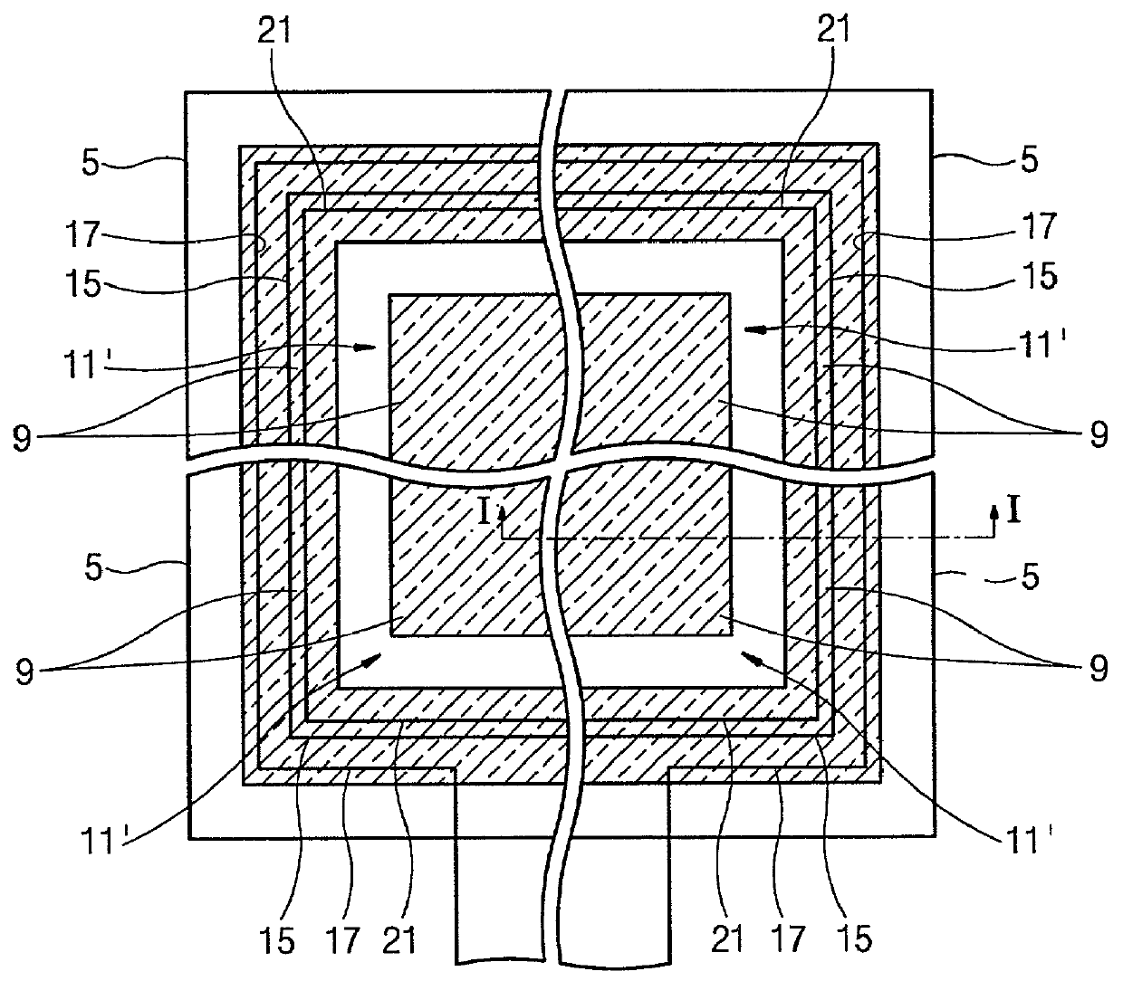
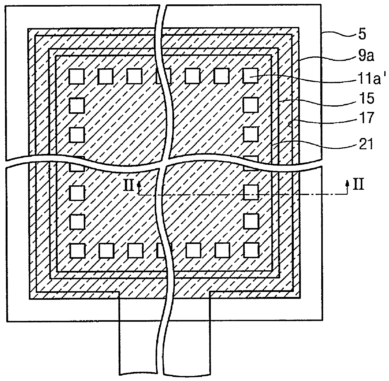
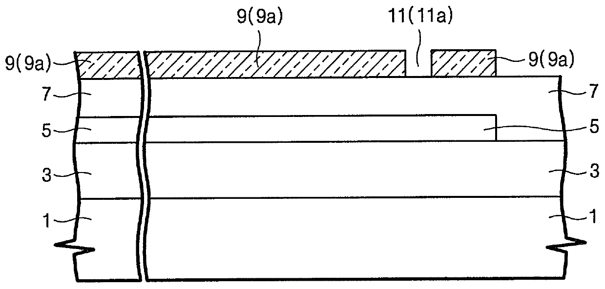
[0023] Referring now to FIGS. 1 and 2, a first conductive layer pattern 5 is stacked on a first insulating layer covering an entire surface of a semiconductor substrate. The first conductive layer pattern 5 is formed from a polysilicon layer or a polycide layer. A second insulating layer (not shown in these figures) covers the resultant structure. A predetermined portion of the second insulating layer is covered with a second conductive layer pa...
PUM
 Abstract
Description
Claims
Application Information