Pixel arrangement evaporation method and pixel arrangement display device capable of improving color gamut and pixels per inch (PPI)

a technology of pixel arrangement and evaporation method, which is applied in the direction of vacuum evaporation coating, solid-state devices, coatings, etc., can solve the problems of increasing the difficulty in controlling the fmm manufacturing process and the oled evaporation process, affecting the evaporation of organic light-emitting materials to form finely colored pixel patterns, and difficult mask processing

Pending Publication Date: 2022-09-29
WUHAN CHINA STAR OPTOELECTRONICS SEMICON DISPLAY TECH CO LTD
View PDF7 Cites 0 Cited by
  • Summary
  • Abstract
  • Description
  • Claims
  • Application Information

AI Technical Summary

Benefits of technology

The patent application is about a new pixel arrangement display device and a method for evaporating pixels. These improvements can enhance the color gamut and PPI (pixels per inch) of OLED screens. The device has larger openings and connection bridges, which are easier to process and less deformed, which can improve productivity and yield. By increasing the distance between pixels, color mixing is avoided and product yield is improved. The method also has larger alignment margin and reduces FMM replacement frequency, leading to increased productivity and reduced cleaning loss. Overall, the device and method improve device resolution, operability, and display quality at a low cost and stability.

Problems solved by technology

With an increase of market demand for high resolution, a diameter of FMM pixel openings is getting smaller and smaller, which greatly increases difficulty in controlling the FMM manufacturing process and the OLED evaporation process.
When the resolution reaches more than 300 ppi, this arrangement requires that the opening and the connecting bridge (the ribs connecting adjacent openings) of the fine metal mask (FMM) are very small, which makes the mask processing difficult.
Further, the alignment accuracy of mask, the shadow of mask, and the deformation of MASK due to other factors will seriously affect the evaporation of organic light-emitting materials to form a finely colored pixel pattern.
However, these new technologies still have many shortcomings, and currently cannot be used for mass production or low yield during mass production.
For example, the need to increase the number of manufacturing processes and additional manufacturing processes results in lower production efficiency; the need to increase equipment and raw materials, and even need to develop special raw materials, resulting in increased investment and costs.
Even so, it is still difficult for these new technologies to produce ultra-high resolution displays above 450 ppi.
At the same time, small FMM pixel openings will also increase the frequency of FMM cleaning in the continuous evaporation process, resulting in reduced production capacity, waste of evaporation materials, and loss of FMM due to increased cleaning times.

Method used


Image

  • Pixel arrangement evaporation method and pixel arrangement display device capable of improving color gamut and pixels per inch (PPI)
  • Pixel arrangement evaporation method and pixel arrangement display device capable of improving color gamut and pixels per inch (PPI)
  • Pixel arrangement evaporation method and pixel arrangement display device capable of improving color gamut and pixels per inch (PPI)

Examples


embodiment 1

[0033]As shown in FIG. 8, this embodiment discloses a pixel arrangement evaporation method capable of improving color gamut and PPI, which includes the following steps:

[0034]a step S1 of using adjacent-closely pixels with same appearance and color on an evaporation substrate as independent units;

[0035]a step S2 of setting number of sub-pixels of each of the independent units to 3N+1 or 3N+2, where N is a positive integer;

[0036]a step S3 of setting fine metal mask (FMM) openings on the evaporation substrate; and

[0037]a step S4 of evaporating all of pixel arrangement methods set in the step S2 and a same unit to form a film by using an evaporation method of a same FMM opening.

[0038]In the step S4, an evaporation zone is included during evaporation, and the evaporation zone is provided with an evaporation unit, an evaporation source, and an evaporation mask. The evaporation source is provided with evaporation source openings, each of evaporation source openings emits evaporation partic...

embodiment 2

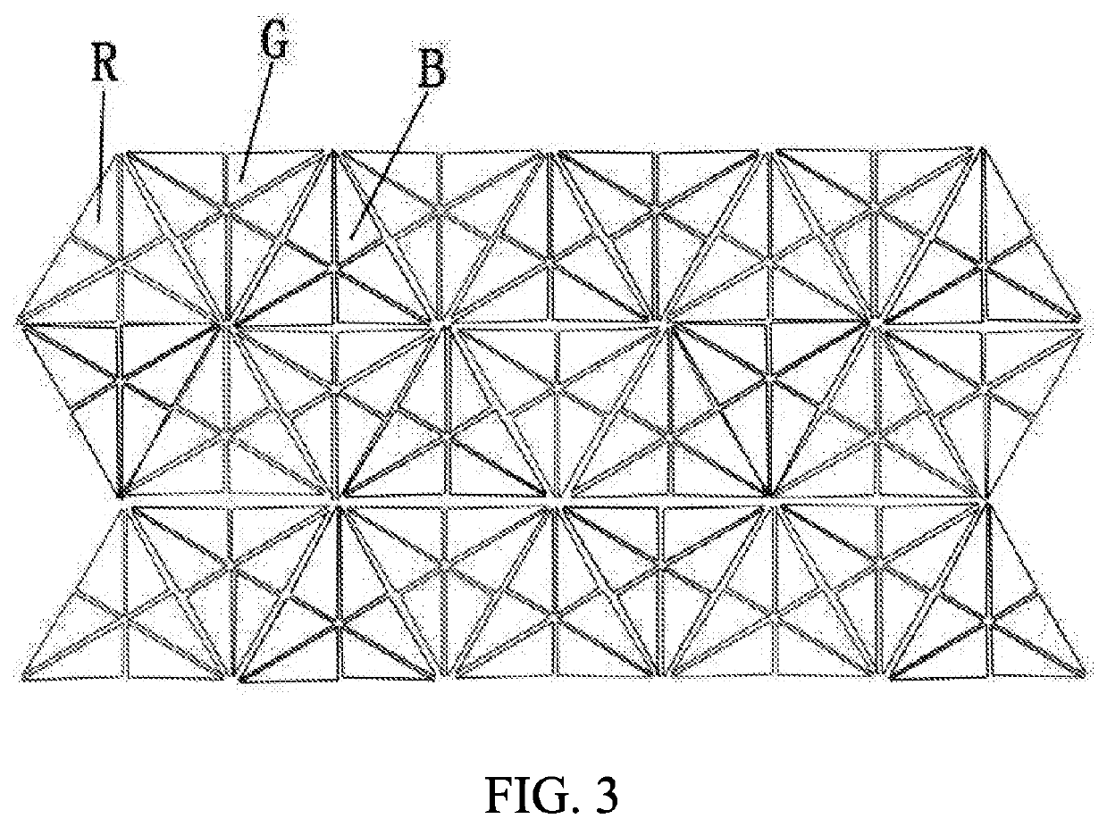
[0042]The present embodiment discloses a pixel arrangement design and an evaporation method for a high color gamut and high PPI OLED device, as shown in FIG. 2. An object is that, when producing OLED screens with the same resolution in this application, the mask of R, G, and B pixels is easier to process and less deformed than the mask of the existing FMM technology because of the larger width of the opening and the connecting bridge. The increase in distance between different pixels is beneficial to avoid color mixing, which is beneficial to improve product yield, larger evaporation alignment margin, easier evaporation process, lower FMM replacement frequency leading to increased productivity, and reduced FMM cleaning loss. Or in other words, in the case that the width of the mask opening is the same as that of the existing FMM technology, the FMM connection bridge is wider and is not easily deformed, which can produce an OLED display with a higher pixel density and a higher color ...

embodiment 3

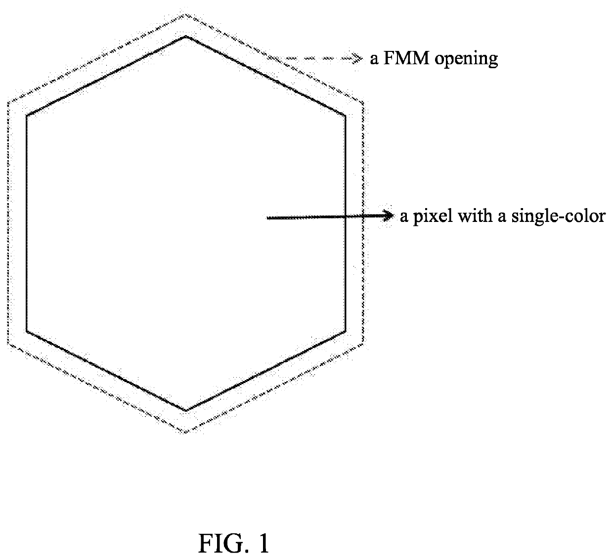
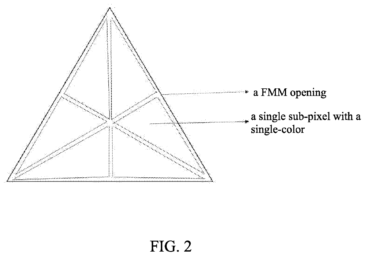
[0045]The present embodiment discloses a pixel arrangement display device and an evaporation method capable of improving color gamut and PPI. On an evaporation substrate, an R pixel, a G pixel, and a B pixel that are triangular in shape, independently controllable, and light-emitting are sequentially arranged on the evaporation substrate, wherein adjacent-closely pixels with same appearance and color on an evaporation substrate are used as independent units, wherein number of the pixels in three single-color independent units can be the same in the independent units arranged in a same row. Number of sub-pixels of each of the independent units to 3N+1 or 3N+2, where N is a positive integer, wherein all of pixel arrangement methods and a same unit are evaporated to form a film by using an evaporation method of a same FMM opening.

[0046]The FMM openings are shown in FIG. 6 and FIG. 7. Shape of the FMM openings is a triangle or a polygon other than a triangle.

[0047]The arrangement design...


PUM

PropertyMeasurementUnit
Gamut indexaaaaaaaaaa
Coloraaaaaaaaaa
Shapeaaaaaaaaaa

Abstract

A pixel arrangement evaporation method and a pixel arrangement display device capable of improving color gamut and pixels per inch (PPI) are provided. On an evaporation substrate, an R pixel, a G pixel, and a B pixel that are triangular in shape, independently controllable, and light-emitting are sequentially arranged on the evaporation substrate. Adjacent-closely pixels with same appearance and color on an evaporation substrate are used as independent units. Number of pixels in three single-color, independent units arranged in a row can be the same. Number of sub-pixels of each of the independent units is 3N+1 or 3N+2, where N is a positive integer. A same unit is vapor-deposited into a film by using an evaporation method of a same fine metal mask (FMM) opening.

Description

FIELD OF INVENTION[0001]The present application relates to organic light-emitting diode (OLED) device manufacturing, and in particular, to a pixel arrangement evaporation method and a pixel arrangement display device capable of improving color gamut and pixels per inch (PPD.BACKGROUND OF INVENTION[0002]In recent years, the use of flat-panel displays in various products and fields requires the flat-panel displays to be further increased in size, high in image quality, and low in power consumption. Under such conditions, an organic electroluminescence (EL) display device including an organic EL device utilizing EL of an organic material is an all-solid-state type which is excellent in low-voltage driving, high-speed response, and spontaneous optical rotation. Flat panel displays have received a lot of attention.[0003]At present, most OLED devices are manufactured with a fine metal mask (FMM) for RGB pixel EL film evaporation. Each FMM opening corresponds to a pixel. The existing mass ...

Claims


Application Information

Patent Timeline
IPC IPC(8): H01L27/32H01L51/00
CPCH01L27/3216H01L51/0011C23C14/042C23C14/24H10K59/353H10K71/164H10K71/166H10K71/00H10K59/121H10K59/352
Inventor HE, RUITING
Owner WUHAN CHINA STAR OPTOELECTRONICS SEMICON DISPLAY TECH CO LTD
Why Eureka
Try Eureka