Micro light-emitting element and display device

A technology for light-emitting components and display devices, which is applied to electrical components, semiconductor devices, electric solid-state devices, etc., can solve the problems of reducing the alignment accuracy of light-emitting diode chips and external circuits, and not having enough alignment margin, and achieves large alignment. Bit margin, the effect of improving alignment accuracy

Active Publication Date: 2022-01-25
PLAYNITRIDE
View PDF4 Cites 0 Cited by
  • Summary
  • Abstract
  • Description
  • Claims
  • Application Information

AI Technical Summary

Problems solved by technology

However, the contact area between the above-mentioned conductive material and the LED chip is smaller than the area of ​​the LED chip, so there is not enough alignment margin between the above-mentioned conductive material and the pad of the external circuit, thus reducing the contact between the LED chip and the external circuit. Alignment accuracy between

Method used


Image

  • Micro light-emitting element and display device
  • Micro light-emitting element and display device
  • Micro light-emitting element and display device

Examples


Embodiment Construction

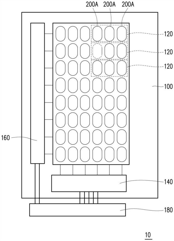
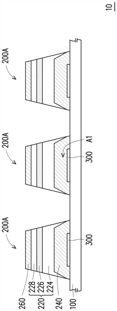
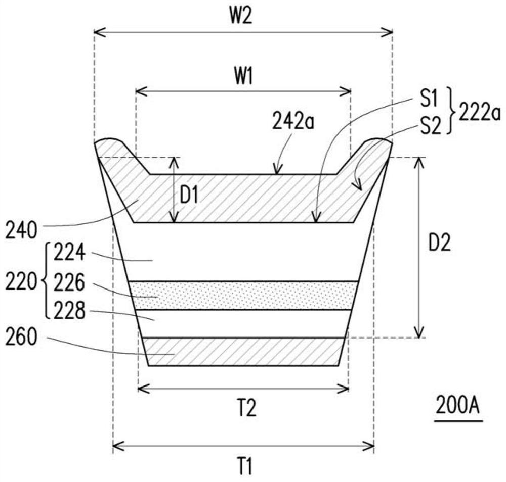
[0060] Figure 1A A schematic top view of a display device according to an embodiment of the present invention is shown. Figure 1B shown as Figure 1A A partial cross-sectional schematic diagram of the display device. Figure 1C A schematic diagram of a micro light-emitting element as an embodiment of the present invention is shown. Please also see Figure 1A , Figure 1B and Figure 1C, the display device 10 of this embodiment includes a driving substrate 100 , a plurality of micro light emitting elements 200A and a plurality of bonding pads 300 . The micro-light emitting elements 200A and the bonding pads 300 are dispersedly disposed on the driving substrate 100 , and the micro-light-emitting elements 200A correspond to the bonding pads 300 respectively. Each micro-light emitting device 200A includes an epitaxial structure layer 220 , a first-type electrode 240 and a second-type electrode 260 . The epitaxial structure layer 220 has a first receiving groove 222a. The fi...


PUM


Abstract

The invention provides a micro light-emitting element and a display device. The micro light-emitting element includes an epitaxial structure layer, a first-type electrode and a second-type electrode. The epitaxial structure layer has a first accommodating groove. The first-type electrode is arranged on the first accommodation groove of the epitaxial structure layer, and has a second accommodation groove. The second type electrode is arranged on the epitaxial structure layer, wherein the epitaxial structure layer is located between the first type electrode and the second type electrode.

Description

technical field [0001] The invention relates to a semiconductor element and an electronic device, in particular to a micro light-emitting element and a display device. Background technique [0002] In general, the light emitting diode chip can be electrically connected to an external circuit by wire bonding or flip-chip bonding. In the case of flip-chip bonding, the electrodes of the LED chip can be electrically connected to the pads on the external circuit through conductive materials such as conductive bumps, conductive paste, and solder. . However, the contact area between the above-mentioned conductive material and the LED chip is smaller than the area of ​​the LED chip, so there is not enough alignment margin between the above-mentioned conductive material and the pad of the external circuit, thus reducing the contact between the LED chip and the external circuit. Alignment accuracy between. Contents of the invention [0003] The invention provides a micro light-em...

Claims


Application Information

Patent Timeline
Patent Type & Authority Patents(China)
IPC IPC(8): H01L33/18H01L33/02H01L27/15
CPCH01L27/153H01L33/02H01L33/18
Inventor 吴志凌苏义闵
Owner PLAYNITRIDE
Why Eureka
Try Eureka