Method for making cover screen type read only memory

A technology of read-only memory and manufacturing method, which is applied in semiconductor/solid-state device manufacturing, electrical components, circuits, etc., and can solve problems such as inconsistent size of coding openings and misalignment of coding openings

Inactive Publication Date: 2004-07-28
MACRONIX INT CO LTD
View PDF0 Cites 1 Cited by
  • Summary
  • Abstract
  • Description
  • Claims
  • Application Information

AI Technical Summary

Problems solved by technology

[0008] The purpose of the present invention is to provide a method for manufacturing a mask-type read-only memory, which can solve the problems arising from misalignment of the code openings in the code area due to misalignment when making the code mask
[0009] Another object of the present invention is to provide a method for manufacturing a mask-type read-only memory, which can solve the problems arising from the inconsistency of the size of the code opening when making the code mask

Method used


Image

  • Method for making cover screen type read only memory
  • Method for making cover screen type read only memory
  • Method for making cover screen type read only memory

Examples


Embodiment Construction

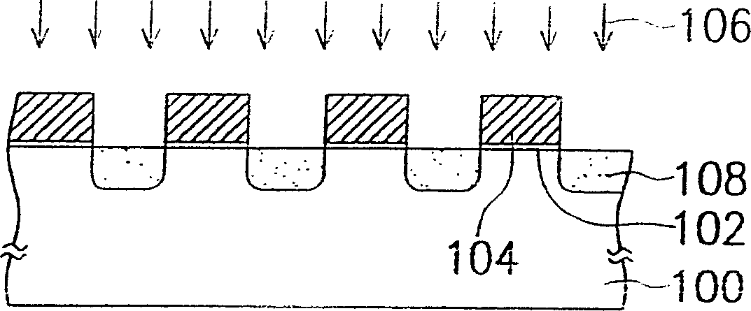
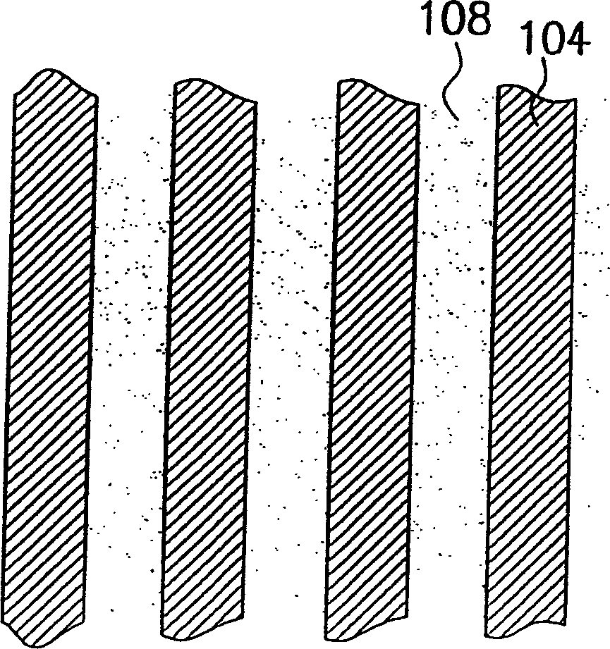
[0030] Please refer to figure 1 , forming a gate dielectric layer 102 and a plurality of conductor lines 104 on a substrate 100 . The forming method of the gate dielectric layer 102 is, for example, a thermal oxidation method. The material of the conductor line 104 is, for example, doped polysilicon, and the forming method is, for example, chemical vapor deposition. Thereafter, ion implantation 106 is performed using the conductor lines 104 as a mask to form a plurality of buried bit lines 108 in the substrate 100 . The ions implanted by ion implantation 106 are, for example, n-type ions, and the top view of its components is as follows figure 2 shown.

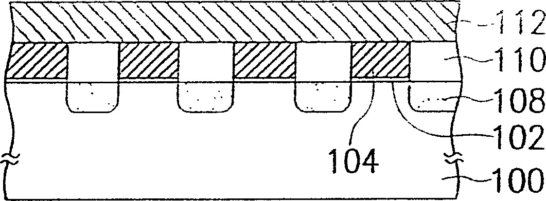
[0031] Next, please refer to image 3 A dielectric layer 110 is filled between the conductor lines 104 , and then, a conductor layer 112 is covered on the dielectric layer 110 and the conductor lines 104 . The material of the dielectric layer 110 is, for example, silicon oxide, and the method of forming it is, for examp...


PUM


Abstract

The invention provides an overcurtained type ROM making method, firstly forming the embedded bit line in the substrate and forming the grid and the word line on the substrate, then forming a precoding layer with plural precoding mouths; then filling these precoding mouths with a filling layer and then forming a coding over curtain on the substrate; then, fully eliminating the filling layer; then removing the coding over curtain, using the precoding and filling layers as mask to make coding ion embedding so as to remove the embedded ions in the coding region.

Description

technical field [0001] The present invention relates to a manufacturing method of a memory, and in particular to a manufacturing method of a mask read-only memory (Mask ROM). Background technique [0002] Mask read-only memory can save data and the saved data will not disappear due to power interruption. It is a storage element widely used in computers and electrical products. In the known manufacturing method of mask type read-only memory, before receiving an order, a semi-finished product that has completed the manufacturing process of embedded bit lines and word lines is produced, and after receiving the order, the photomask is manufactured according to the requirements of the order To carry out coding (coding), in order to make the required mask type ROM products. [0003] In a typical encoding step, a layer of photoresist is first formed on the substrate, and then exposed with a photomask made according to the order requirements. After the photoresist is developed, th...

Claims


Application Information

Patent Timeline
Patent Type & Authority Applications(China)
IPC IPC(8): H01L21/8246
Inventor 钟维民
Owner MACRONIX INT CO LTD
Why Eureka
Try Eureka