

Solid-state image sensor, method for manufacturing the same, and camera
- Summary
- Abstract
- Description
- Claims
- Application Information
AI Technical Summary
Benefits of technology
Problems solved by technology
Method used
Image

Examples
Embodiment Construction
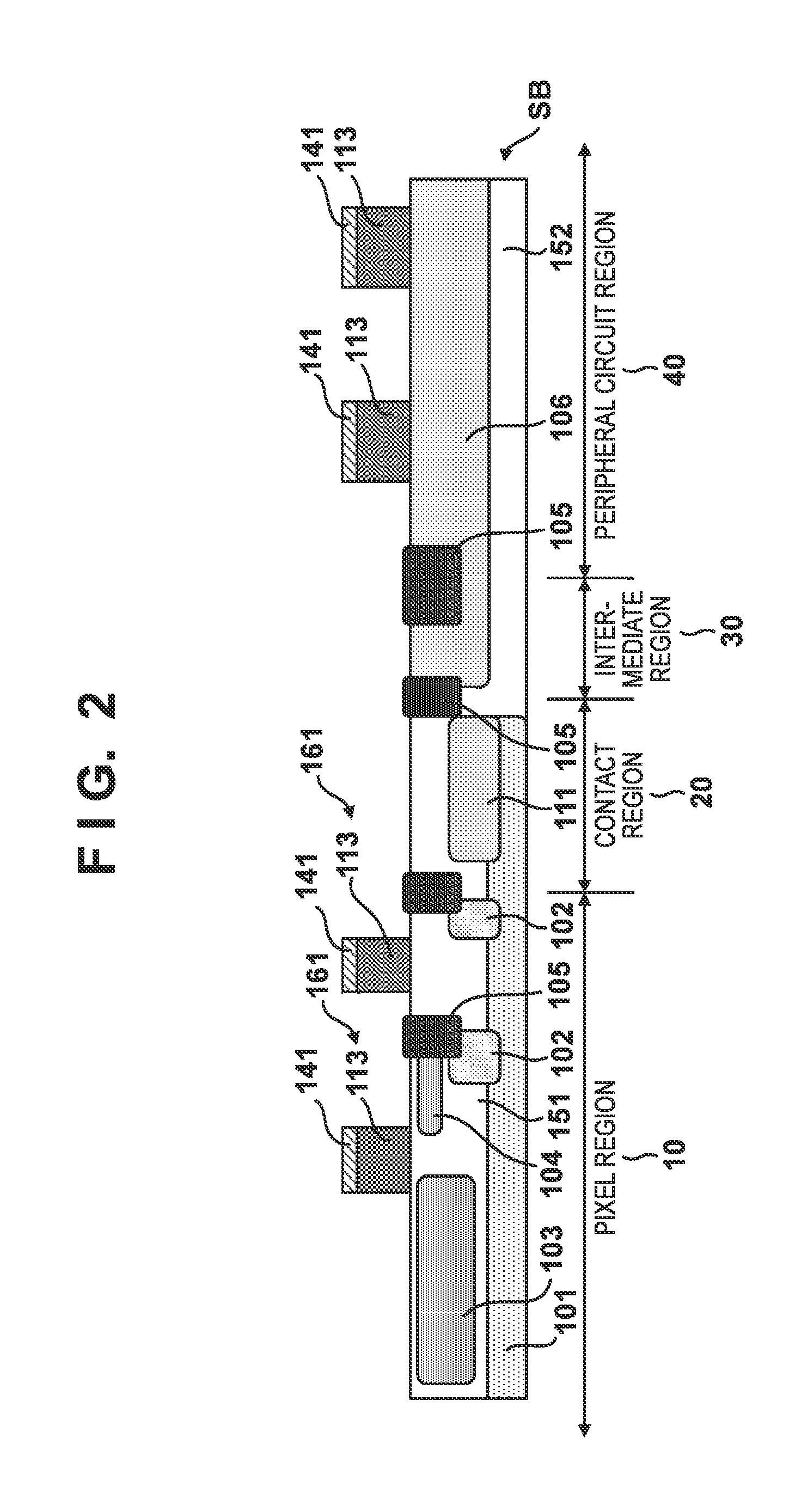
[0013]A preferred embodiment of the present invention will now be described with reference to the accompanying drawings. A case in which a silicide is used to increase the operation speed of a transistor will be exemplified. However, the present invention is not limited to this, and it suffices to form a compound (high melting point metal compound) of a material forming an active region, and a high melting point metal. Examples of a semiconductor material forming an active region are silicon and gallium arsenide. Examples of the high melting point metal are cobalt, tungsten, and titanium. As for an etch stop film, a case in etching stops at the etch stop film will be explained. However, etching need not completely stop, and it is only necessary to decrease the etching rate by arranging a low-etching-rate film for a film to be etched.
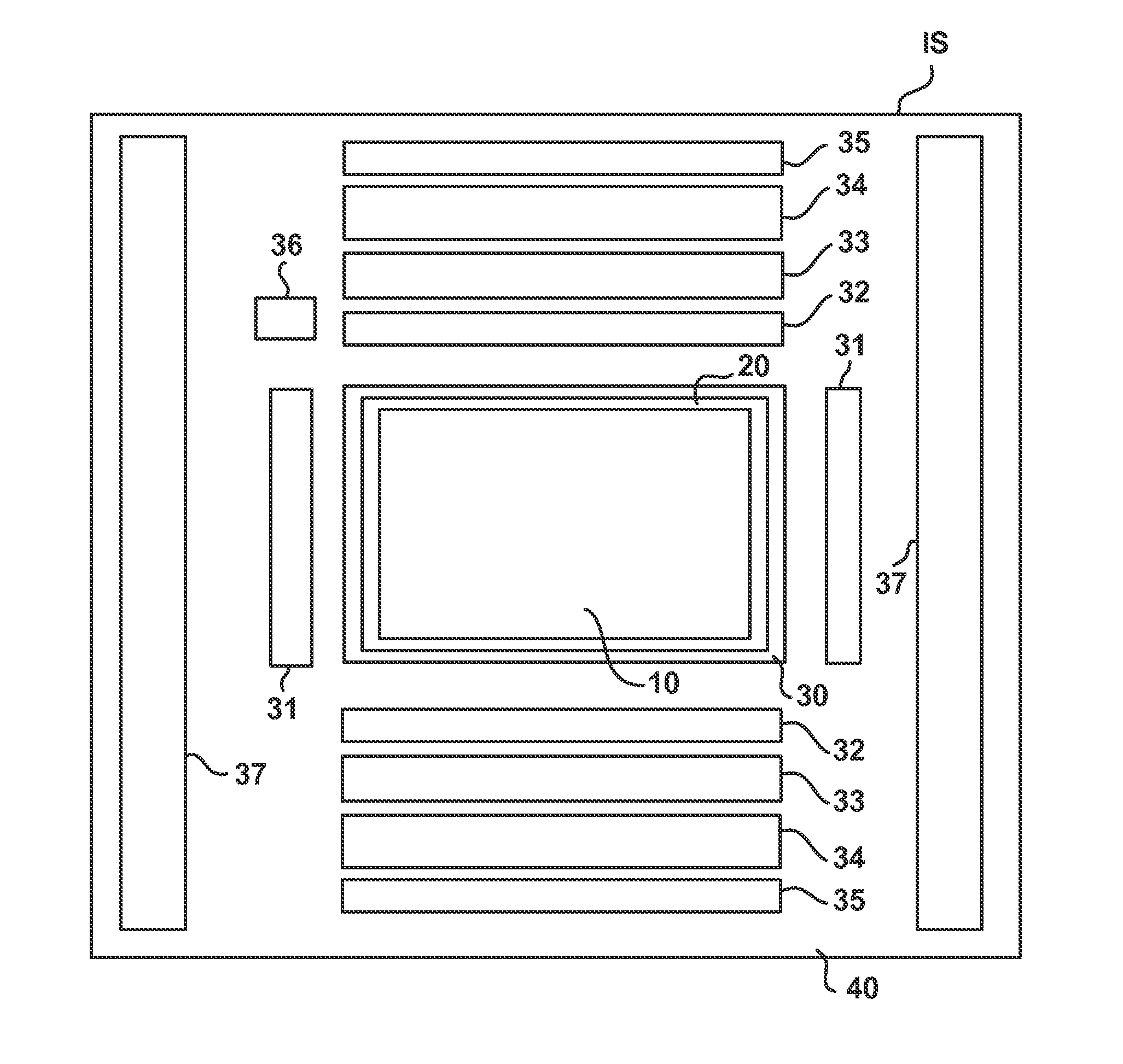
[0014]FIG. 1 is a plan view schematically showing the arrangement of a solid-state image sensor IS according to an embodiment of the present invention. ...
PUM
 Abstract
Description
Claims
Application Information