Apparatus and methods for coverlay removal and adhesive application

Inactive Publication Date: 2005-02-17
MICRON TECH INC
View PDF40 Cites 9 Cited by
  • Summary
  • Abstract
  • Description
  • Claims
  • Application Information

AI Technical Summary

Benefits of technology

[0008] When functional dice are attached to the “reject die sites” of the support element and further are processed, the resulting semiconductor packages are necessarily defective. This sacrifices functional dice, thereby increasing semiconductor package manufacturing costs and decreasing yields. To avoid the added cost (i.e., sacrificing functional dice), a “reject die site” on a support element could simply be skipped or omitted during the die attach process. Regrettably, omitting attachment of a die to a die site on a support element causes problems during the encapsulation process.
[0009] During the encapsulation process, liquid encapsulation material flows over and around the attached dice and substrates of the support element. If one or more bonding slots are left open, i.e., a die is not attached to a die site of the support element, the encapsulation material flows through the uncovered opening 26. When the encapsulation material flows through such openings, it contaminates dice adjacent and/or near the uncovered opening. This is known as “bleeding or flashing.” The bleeding of encapsulation material produces even more defective semiconductor packages, further increasing manufacturing costs and lowering yield. Moreover, bleeding of the encapsulation material may stick to the mold body and contaminate the next support element processed through the encapsulation machine.
[0010] In attempt to avoid (1) sacrificing functional dice by attaching the dice on reject die sites (2) contaminatin gadjacent dice and mold bodies by omitting attachment of dice to reject die sites, and (3) processing support elements that include a minimal number of substrates due to prior separation of the defective substrates, the industry pays a premium price for support elements having no reject die sites. This also increases semiconductor package manufacturing costs.
[0011] Accordingly, there is a need for a process for making semiconductor packages using support elements having one or more reject die sites without contaminating adjacent dice and

Problems solved by technology

Currently available support elements typically include one or more substrates that are defective or non-functional, i.e., the substrates include “reject die sites.” Individual substrates of a support element may be non-functional for a variety of reasons, such as faulty electrical circuitry of a substrate.
Such defect substrates of the support element cannot be utilized to fabricate a functional semiconductor package but cannot be separated from the support element prior to processing of the other substrates on the support element.
If the defective substrates are separated from the support element, such action necessarily limits the number of substrates that may be processed at one time using the separated support element.
When functional dice are attached to the “reject

Method used


Image

  • Apparatus and methods for coverlay removal and adhesive application
  • Apparatus and methods for coverlay removal and adhesive application
  • Apparatus and methods for coverlay removal and adhesive application

Examples


Embodiment Construction

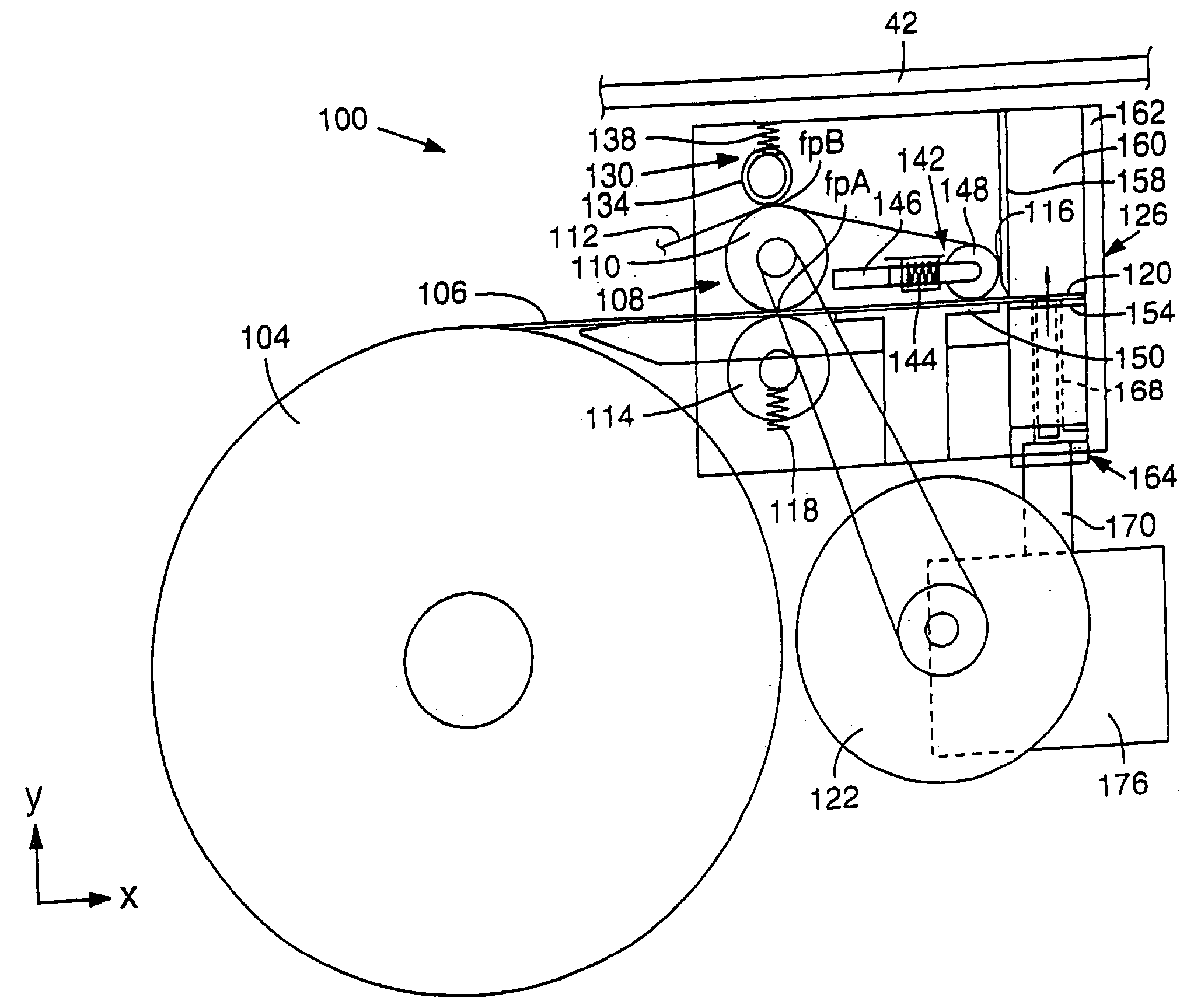
[0019] The present invention provides apparatus and methods for attachment of an adhesive strip as a cover member on one or more reject die sites 36 of semiconductor package support elements 42 (FIG. 2a and 2B). The apparatus and method of the present invention synchronously remove a coverlay film from a reel of adhesive film as it cuts and applies exact lengths of adhesive to the support element.

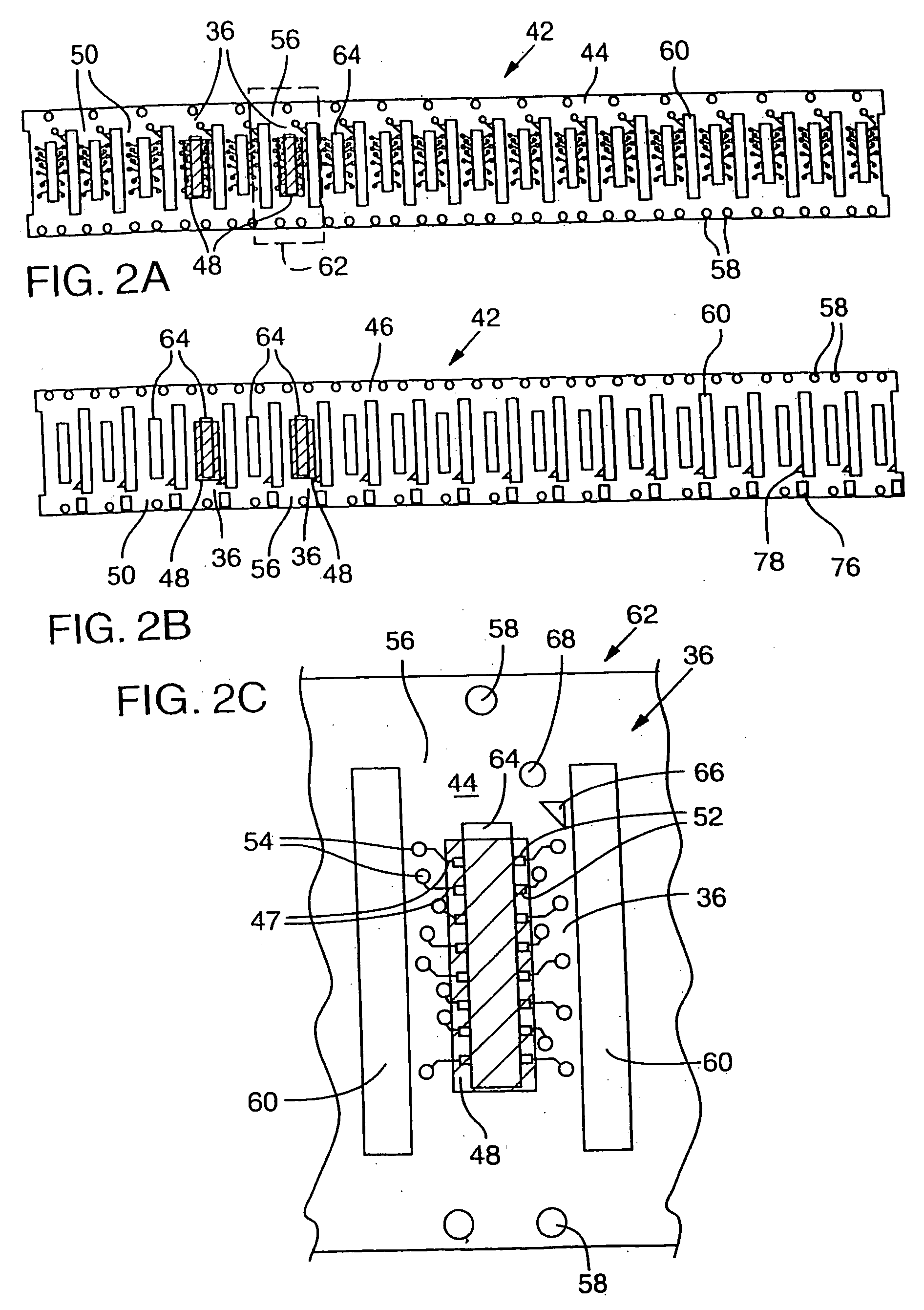
[0020] With reference to FIGS. 2A-2C, a representative support element 42 includes multiple substrates 56. Each substrate 56 is a segment of the support element 42 and will subsequently be separated from the adjacent substrates 56. The support element shown in FIGS. 2A and. 2B includes 18 substrates 56. However, this number is merely exemplary and the support element 42 may include a fewer or greater number of substrates 56. The substrates 56 are typically positioned side-by-side and are integrally connected. As stated above, the support element 42 facilitates the fabrication process in th...


PUM

PropertyMeasurementUnit
Fractionaaaaaaaaaa
Fractionaaaaaaaaaa
Lengthaaaaaaaaaa

Abstract

Apparatus and methods for synchronously removing coverlay film from an adhesive film and applying an adhesive strip cut from the adhesive film to cover one or more reject die sites and/or functional die sites on semiconductor package support elements are disclosed. Reject die sites on defective substrates are covered prior to encapsulation.

Description

FIELD OF THE INVENTION [0001] This invention relates generally to apparatus and methods for semiconductor package fabrication and more specifically to apparatus and methods for synchronous coverlay film removal and adhesive application to semiconductor support elements and the like. BACKGROUND AND SUMMARY OF THE INVENTION [0002] In semiconductor manufacture, a single semiconductor die (or chip) can be packaged within a sealed package. The package protects the die from damage and from contaminants in the surrounding environment. In addition, the package provides a substantial lead system for electrically connecting the integrated circuits on the die to the outside world. [0003] One type of semiconductor package 10 is illustrated in FIG. 1A. The package 10 includes a substrate 12 having a planar die attach surface or die site 22. A semiconductor die 16 is mounted to an upper surface of the substrate 12 on the die site 22. The die 16 is typically adhesively bonded to the substrate 12 w...

Claims


Application Information

Patent Timeline
IPC IPC(8): B65H35/00B65H37/00H01L21/00H01L23/498
CPCB65H35/0013Y10T156/1062H01L21/67132H01L23/4985H01L2224/4824H01L2924/14Y10T156/1339Y10T156/16Y10T156/1074Y10T156/1322Y10T156/1105Y10T156/17Y10T156/1335Y10T156/107Y10T156/1326B65H37/002
Inventor PRINDIVILLE, CASEY
Owner MICRON TECH INC
Why Eureka
Try Eureka