Semiconductor device

a technology of semiconductor devices and semiconductors, applied in the direction of semiconductor devices, electrical devices, transistors, etc., can solve the problems of reducing the yield of products and adversely affecting the characteristics of elements, so as to improve the yield and reliability of semiconductor devices, prevent the damage of elements, and improve the effect of semiconductor device performan

Inactive Publication Date: 2008-03-27
SEMICON ENERGY LAB CO LTD
View PDF13 Cites 9 Cited by
  • Summary
  • Abstract
  • Description
  • Claims
  • Application Information

AI Technical Summary

Benefits of technology

[0019]Even when the semiconductor device is stressed in the manufacturing process of the semiconductor device or utilization after completion thereof, damages of the element can be prevented, and therefore th...

Problems solved by technology

However, when force such as bending is externally applied to a semiconductor device including an integrated circuit provided with an element such as a transistor over a flexible substrate, stress caused in the semiconductor device might damage the element such as a transistor which is ...

Method used


Image

  • Semiconductor device
  • Semiconductor device
  • Semiconductor device

Examples


embodiment mode 1

[0049]In this embodiment mode, an example of the semiconductor device of the present invention is described with reference to drawings.

[0050]The semiconductor device of the present invention has a structure for preventing an element provided in the semiconductor device, such as a transistor, from being damaged even in the case where the semiconductor device is stressed by being applied with force such as bending. In this embodiment mode, as an example of the structure, the case is described in which a film functioning as a protective film is provided above a semiconductor film included in the transistor.

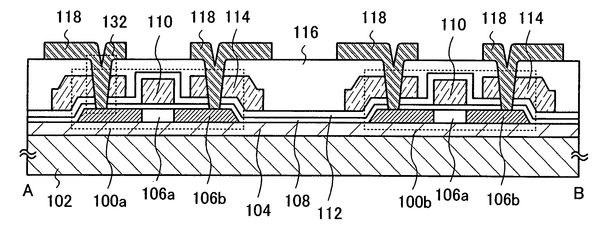
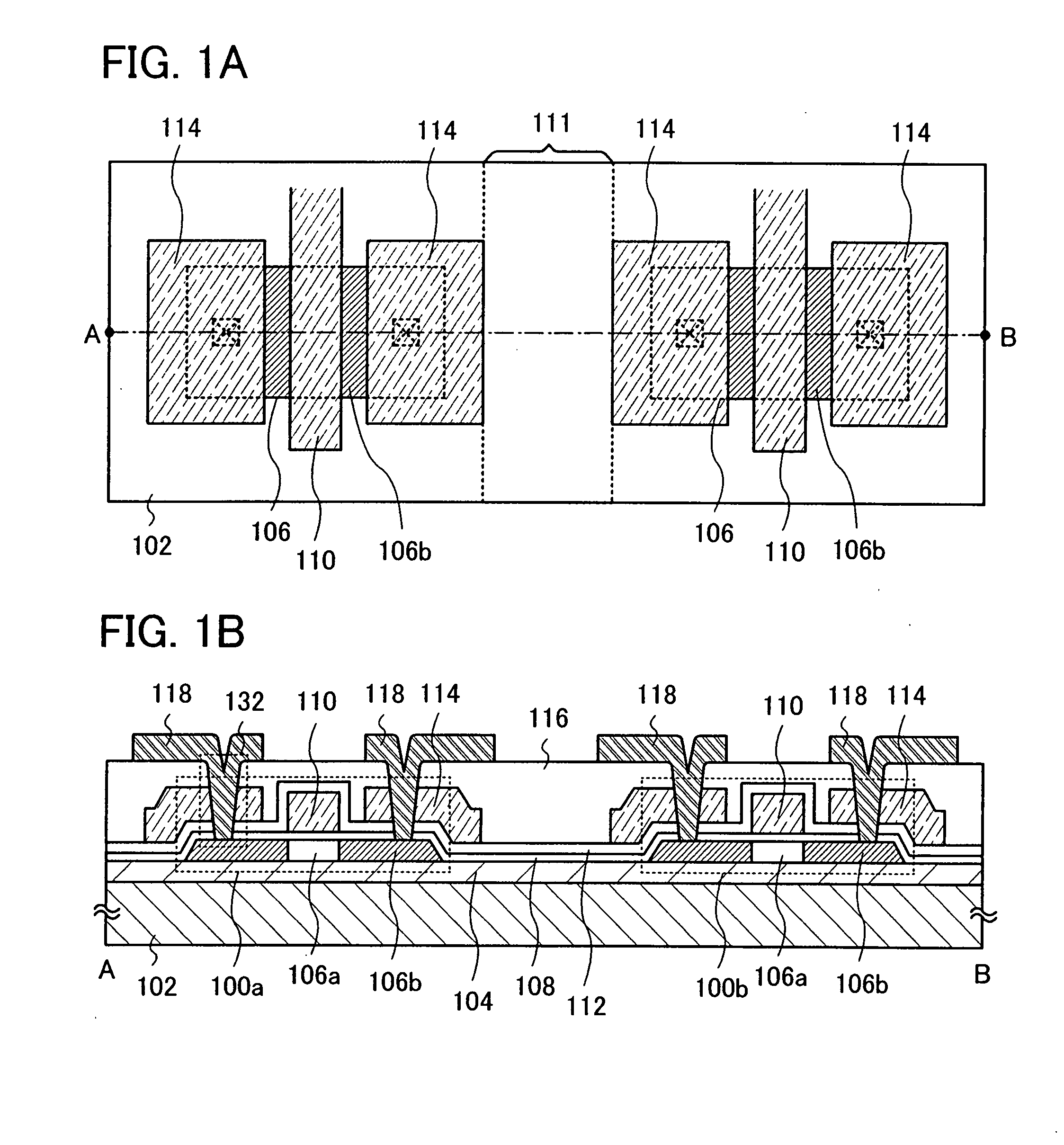
[0051]FIGS. 1A and 1B show an example of the semiconductor device described in this embodiment mode. Note that FIG. 1A shows a top plan view and FIG. 1B shows a cross-sectional view taken along a line A-B in FIG. 1A.

[0052]The semiconductor device shown in FIGS. 1A and 1B includes thin film transistors 100a and 100b each including at least a semiconductor film 106, a gate insulating f...

embodiment mode 2

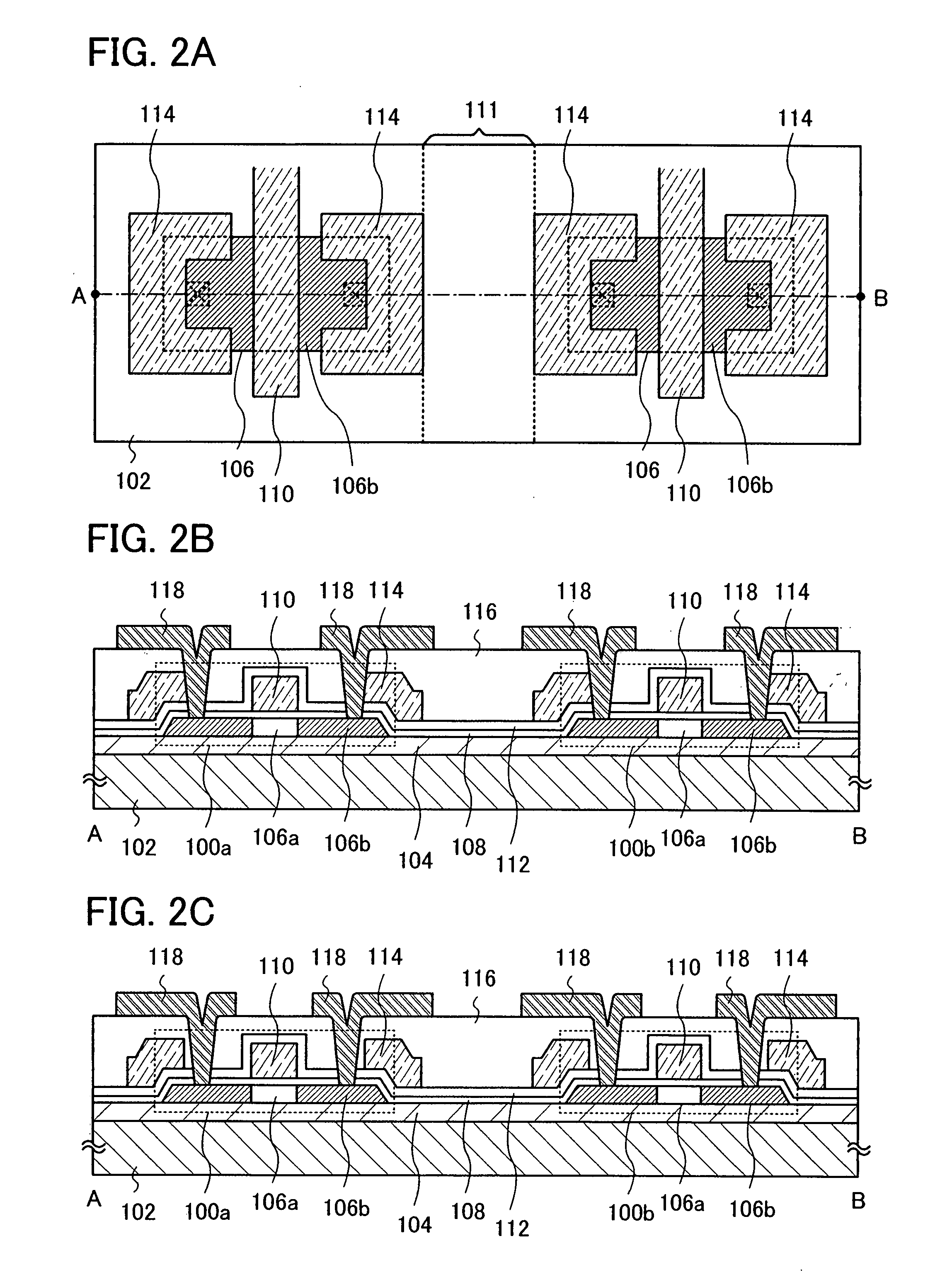
[0069]In this embodiment mode, an example of a method for manufacturing the semiconductor device described in Embodiment Mode 1 is described with reference to drawings. Note that in this embodiment mode, the process is described in which after an element such as a thin film transistor is formed over a supporting substrate, the element is released from the supporting substrate to be transferred to another substrate.

[0070]First, a release layer 122 is formed over one surface of a substrate 120. Subsequently, an insulating film 104 that functions as a base and an amorphous semiconductor film (for example, a film containing amorphous silicon) are formed (see FIG. 4A). Note that the release layer 122, the insulating film 104, and the amorphous semiconductor film can be sequentially formed.

[0071]As the substrate 120, a glass substrate, a quartz substrate, a metal substrate, a stainless steel substrate, or the like can be used. In the case of using such a substrate, the area and the shape ...

embodiment mode 3

[0111]In this embodiment mode, the case where, in a thin film transistor of the semiconductor device described in Embodiment Mode 1 or 2, an insulating film is formed to be in contact with a side surface of the first conductive film functioning as a gate electrode and an LDD region is formed below the insulating film is described with reference to drawings.

[0112]The semiconductor device described in this embodiment mode includes the thin film transistors 100a and 100b, and insulating films 144 are provided to be in contact with a side surface of the first conductive films 110 functioning as gate electrodes, which are included in the thin film transistors 100a and 100b (see FIGS. 7A and 7B). The insulating films 144 are also referred to as side walls, and a structure in which LDD regions are provided below the insulating films 144 can be employed. Note that FIG. 7A shows a structure in FIGS. 1A and 1B in which the insulating films 144 and the impurity regions 106c functioning as LDD ...


PUM


Abstract

An object is to provide a semiconductor device in which damages of an element such as a transistor are reduced even when physical force such as bending is externally applied to generate stress in the semiconductor device. A semiconductor device includes a semiconductor film including a channel formation region and an impurity region, which is provided over a substrate, a first conductive film provided over the channel formation region with a gate insulating film interposed therebetween, a first interlayer insulating film provided to cover the first conductive film, a second conductive film provided over the first interlayer insulating film so as to overlap with at least part of the impurity region, a second interlayer insulating film provided over the second conductive film, and a third conductive film provided over the second interlayer insulating film so as to be electrically connected to the impurity region through an opening.

Description

BACKGROUND OF THE INVENTION[0001]1. Field of the Invention[0002]The present invention relates to a semiconductor device, in particular, a semiconductor device in which damages of an element such as a transistor provided in the semiconductor device are reduced even when a stress is applied.[0003]2. Description of the Related Art[0004]In recent years, a technique for providing an integrated circuit including a transistor or the like over a flexible substrate such as a plastic substrate has attracted attention (for example, Patent Document 1: Japanese Published Patent Application No. 2003-204049). A semiconductor device formed by providing an integrated circuit over a flexible substrate can be reduced in weight, cost, or the like as compared to the case of using a substrate such as a semiconductor substrate or a glass substrate. Since a flexible semiconductor device can be bent for example, it is expected to be applied to various fields and places (For example, Patent Document 2: Japan...

Claims


Application Information

Patent Timeline
IPC IPC(8): H01L29/04H01L29/786
CPCH01L27/1266H01L27/124H01L29/78606H01L29/78603H01L21/18
Inventor ARASAWA, RYOMIYAZAKI, AYAMONOE, SHIGEHARUYAMAZAKI, SHUNPEI
Owner SEMICON ENERGY LAB CO LTD
Why Eureka
Try Eureka