Light emitting diode structure and manufacturing method thereof

a technology of light-emitting diodes and manufacturing methods, which is applied in the direction of semiconductor/solid-state device manufacturing, semiconductor devices, electrical devices, etc., can solve the problems of deteriorating luminous efficiency, pn junction, increasing the time and cost required in the manufacturing process, etc., and achieves the effect of reducing time and cost and high resistan

Inactive Publication Date: 2014-01-02
LEXTAR ELECTRONICS CORP
View PDF5 Cites 6 Cited by
  • Summary
  • Abstract
  • Description
  • Claims
  • Application Information

AI Technical Summary

Benefits of technology

[0009]The invention is directed to a light-emitting diode (LED) structure and a manufacturing method thereof. Through an etching process using photolithography technology and the high resistance between the positive electrode and the junction underneath, the input current is spread and conducted, hence reducing the time and cost required in the manufacturing process

Problems solved by technology

When a voltage is applied so that a current is inputted between the positive (or the p-type) terminal and the negative (or the n-type) terminal to illuminate the PN junction between the P type semiconductor and the N type semiconductor, the elements of the positive electrode may block the light emitted by the PN junction and deteriorate luminous efficiency.
However, the manufacturing method of the LED structure requires one more process for forming the insulating current blocking layer 110, hence increasing the time and cost required in the manufacturing process.

Method used


Image

  • Light emitting diode structure and manufacturing method thereof
  • Light emitting diode structure and manufacturing method thereof
  • Light emitting diode structure and manufacturing method thereof

Examples


first embodiment

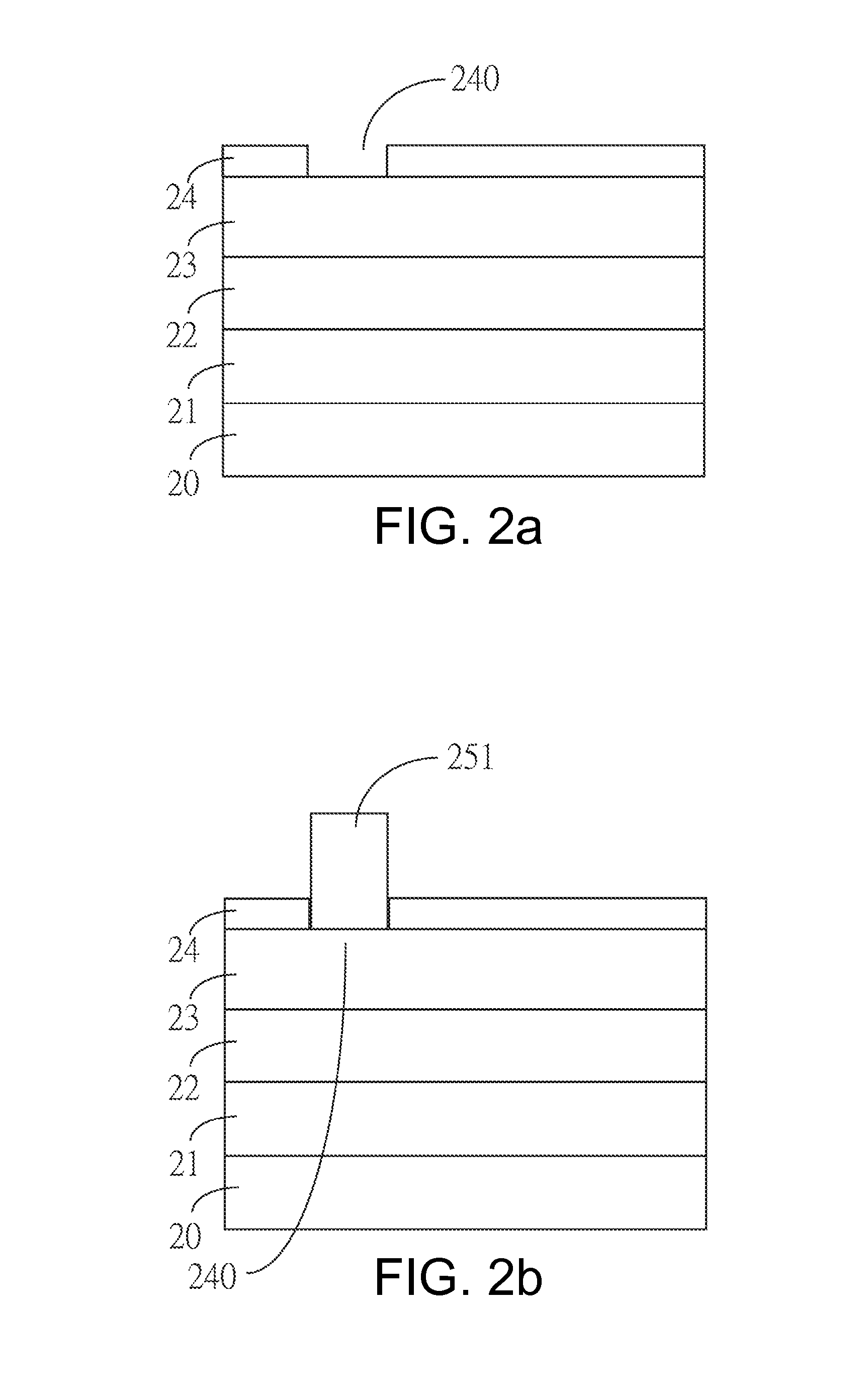
[0025]Therefore, the last configuration of FIG. 2(d) is the light-emitting diode (LED) structure 200 manufactured by the manufacturing method of an LED structure according to the present invention. As illustrated in the diagram, the LED structure 200 includes a semiconductor substrate 20, a first type semiconductor layer 21, a light-emitting layer 22, a second type semiconductor layer 23, an electrode contact layer 24, a positive electrode 251 and a negative electrode 252. The first type semiconductor layer 21 is formed on the semiconductor substrate 20. The light-emitting layer 22 is formed on partial surface of the first type semiconductor layer 21. The second type semiconductor layer 23 corresponds to a top surface of the light-emitting layer 22 and is formed on the light-emitting layer 22. The electrode contact layer 24 having the first opening 240 is formed on the second type semiconductor layer 23 for exposing partial surface of the second type semiconductor layer 23. The posi...

second embodiment

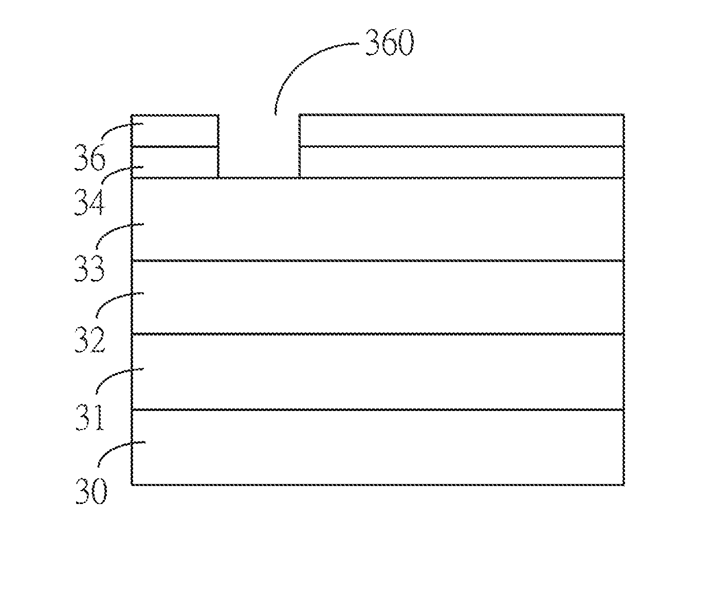
[0033]Referring to FIG. 3(d), a negative electrode 352 is formed on partial exposed surface of the first type semiconductor layer 31. The last configuration of FIG. 3(d) is the light-emitting diode (LED) structure 300 manufactured by the manufacturing method of an LED structure according to the present invention.

[0034]To summarize, the LED structure of the present invention spreads and conducts the inputted current through an etching process using photolithography technology and the high resistance between the positive electrode and the junction underneath. In comparison to the prior art, the present invention not only spreads and conducts the current to effectively increase luminous efficiency, but further simplifies the manufacturing process of forming the insulating current blocking layer and reduces both the required manufacturing time and the cost. Therefore the present invention effectively resolves the problems encountered in the prior art and successfully achieves the main o...


PUM


Abstract

A light-emitting diode structure and a manufacturing method thereof are provided. The structure includes a semiconductor substrate, a first type semiconductor layer, a light-emitting layer, a second type semiconductor layer, an electrode contact layer, a positive electrode and a negative electrode. A stacking layer consisting of the first type semiconductor layer, the light-emitting layer, the second type semiconductor layer and the electrode contact layer is formed on the semiconductor substrate, and a first opening penetrates the electrode contact layer and exposes a part of the second type semiconductor layer. The positive electrode is formed in the first opening. A part of the first type semiconductor layer, the light-emitting layer, the second type semiconductor layer and the electrode contact layer is removed to form a platform structure. The negative electrode is formed on the exposed surface of the first type semiconductor layer.

Description

[0001]This application claims the benefit of Taiwan application Serial No. 101123245, filed Jun. 28, 2012, the subject matter of which is incorporated herein by reference.BACKGROUND OF THE INVENTION[0002]1. Field of the Invention[0003]The invention relates in general to a light-emitting diode (LED) structure and a manufacturing method thereof, and more particularly to an LED structure capable of spreading and conducting the input current and a manufacturing method thereof.[0004]2. Description of the Related Art[0005]Light emitting diode (LED) relates to a solid state light-emitting element made from a semiconductor material. LED, having the features of small volume, low degree of heating generation, high lamination, low power consumption, long lifespan and being suitable for mass production, so the light emitting diode has been widely used as a lighting source for various lighting devices or back light modules. As the application of LED is getting more and more popular, how to incre...

Claims


Application Information

Patent Timeline
Patent Type & Authority Applications(United States)
IPC IPC(8): H01L33/04H01L33/32
CPCH01L33/04H01L33/32H01L33/14H01L33/42
Inventor CHEN, MING-SHENG
Owner LEXTAR ELECTRONICS CORP
Why Eureka
Try Eureka