Storage cell bridge screen technique

a technology of storage cell and screen, applied in the direction of information storage, static storage, digital storage, etc., can solve the problems of memory device malfunction, the bridge formed during the manufacturing process between neighboring memory cells,

Active Publication Date: 2014-01-02
SK HYNIX INC
View PDF2 Cites 10 Cited by
  • Summary
  • Abstract
  • Description
  • Claims
  • Application Information

AI Technical Summary

Benefits of technology

[0012]In another embodiment, the first and second memory cells are connected to a wordline which is selected in the active cycle, and in response to the selection of the wordline, the first and second memory cells cause the first and second bitlines to respectively have first and second voltage levels opposite one another relative to the precharge voltage level.

Problems solved by technology

As semiconductor memory technology continues to advance and the size of memory cells continues to shrink, problems associated with bridges formed during the manufacturing process between neighboring memory cells (e.g., due to manufacturing defects such as conductive particles) become more pronounced.
Such bridges create resistive shorts between neighboring memory cells that can cause the memory device to malfunction.
However, if the bridge results in a more resistive short, detection of such bridge during the wafer or package test becomes more difficult.
Often, such undetected bridges result in premature failure of the part in the field.
However, all these techniques require complex test algorithms and / or extensive on-chip circuitry which lengthen the test time and / or increase the die size.

Method used


Image

  • Storage cell bridge screen technique
  • Storage cell bridge screen technique
  • Storage cell bridge screen technique

Examples


Embodiment Construction

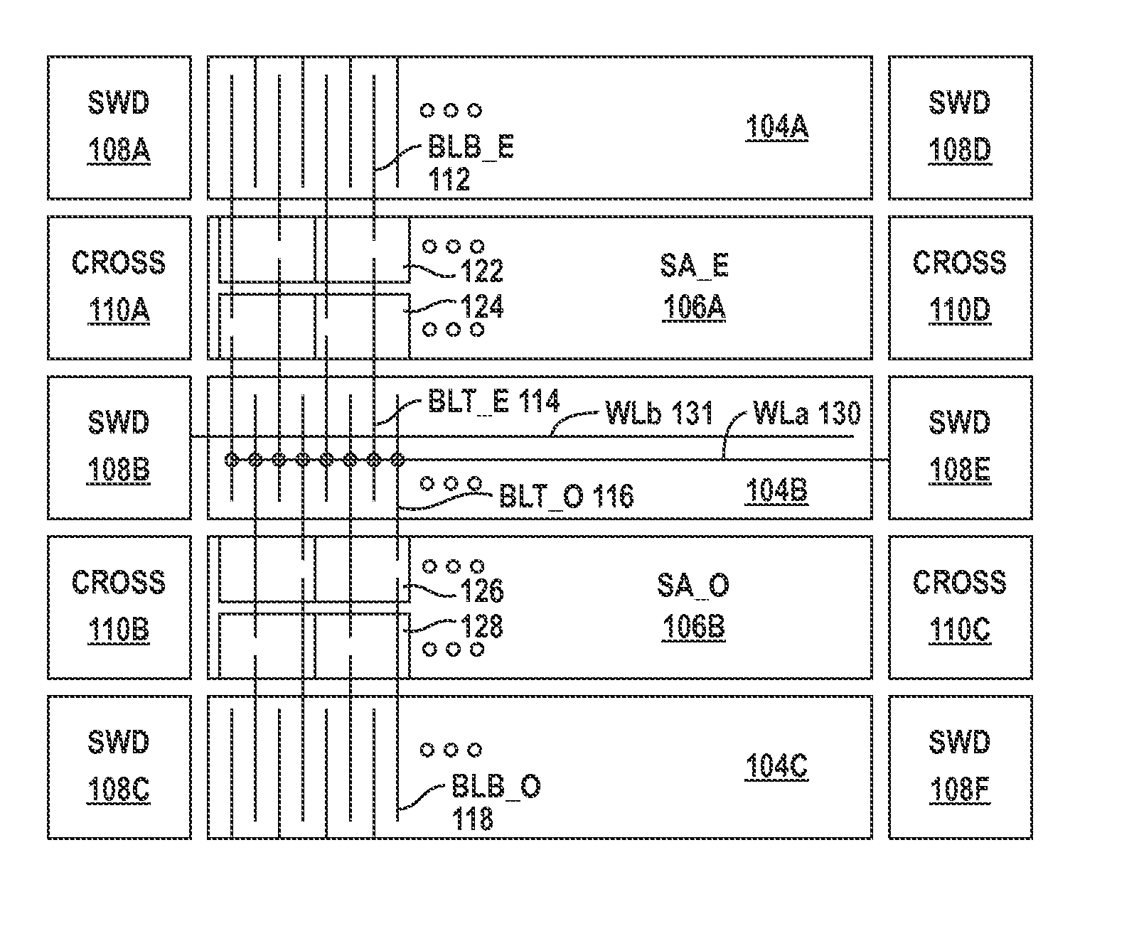
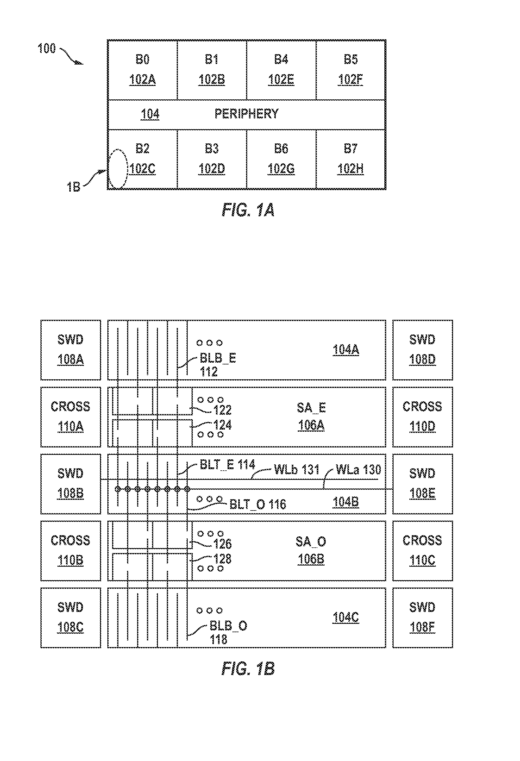
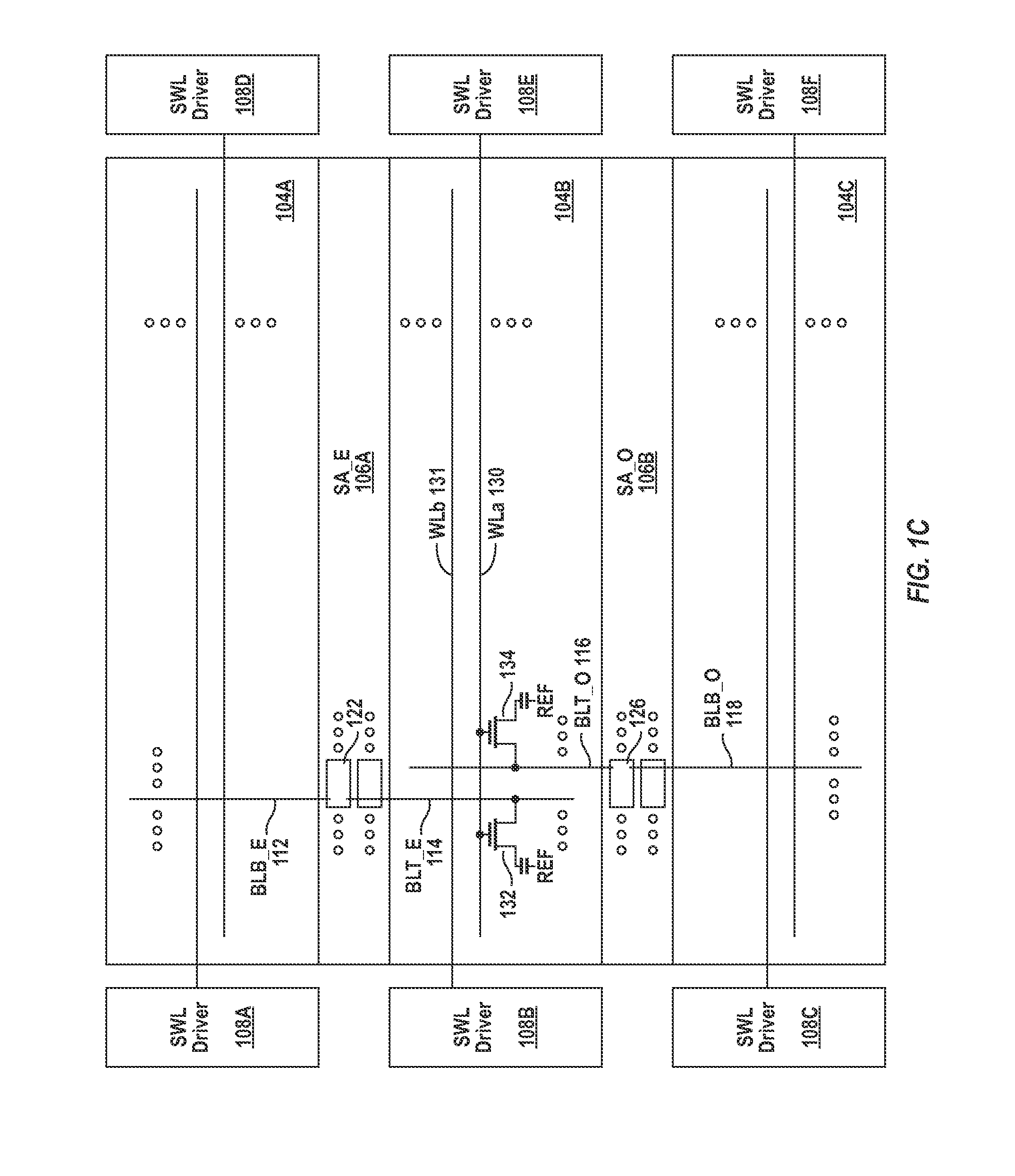
[0023]Bridges between neighboring memory cells in a memory device are detected using a simple but highly effective technique. For illustration purposes only, the bridge screen technique is briefly described in the next paragraph in the context of what is named herein as the “odd bitline stress” condition. Under the “odd bitline stress condition,” a bridge between two neighboring memory cells, one of which is connected to an odd bitline and the other one connected to an even bitline, is detected by causing the even bitline to have a higher potential than the neighboring odd bitline thus causing the odd bitline to lose its potential through the conductive bridge between the two neighboring memory cells. It is noted that the bridge screen technique described herein is equally effective in the context of an “even bitline stress” condition where an odd bitline is caused to have a higher voltage level than a neighboring even bitline.

[0024]During testing, a known data pattern is written in...


PUM


Abstract

A semiconductor memory includes a circuit block that is configured to receive a test mode command, a first sense amplifier that is coupled to sense and amplify a state of a first memory cell when enabled, and a second sense amplifier that is coupled to sense and amplify a state of a second memory cell when enabled. In an active cycle, the circuit block generates one or more control signals in response to the test mode command that cause the second sense amplifier to be enabled a predetermined amount of time after the first sense amplifier is enabled.

Description

BACKGROUND OF THE INVENTION [0001]As semiconductor memory technology continues to advance and the size of memory cells continues to shrink, problems associated with bridges formed during the manufacturing process between neighboring memory cells (e.g., due to manufacturing defects such as conductive particles) become more pronounced. Such bridges create resistive shorts between neighboring memory cells that can cause the memory device to malfunction. Severe ridges between neighboring memory cells can be detected during testing of memory devices and addressed, for example, using row and / or column redundancy techniques. However, if the bridge results in a more resistive short, detection of such bridge during the wafer or package test becomes more difficult. Often, such undetected bridges result in premature failure of the part in the field.[0002]A number of techniques for detecting bridges have been proposed. However, all these techniques require complex test algorithms and / or extensi...

Claims


Application Information

Patent Timeline
Patent Type & Authority Applications(United States)
IPC IPC(8): G11C7/02G11C7/00
CPCG11C7/02G11C7/08G11C29/025
Inventor JUNG, TAEHYUNGKIM, KEESOO
Owner SK HYNIX INC
Why Eureka
Try Eureka