Substrate for semiconductor package and process for manufacturing
a technology of semiconductor packaging and substrate, applied in the direction of printed circuit manufacturing, printed circuit aspects, basic electric elements, etc., can solve the problems of non-coplanar top surfaces of plated pillars, negatively affecting the reliability of solder joints, and non-uniform electric current density distribution
- Summary
- Abstract
- Description
- Claims
- Application Information
AI Technical Summary
Problems solved by technology
Method used
Image

Examples
Embodiment Construction
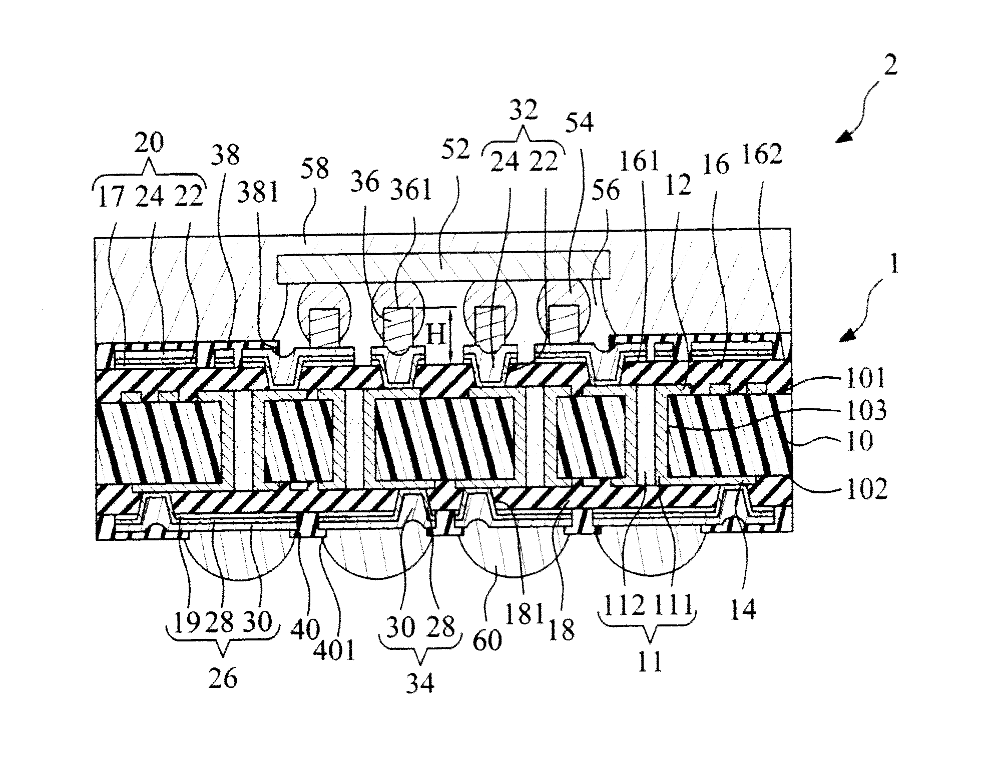
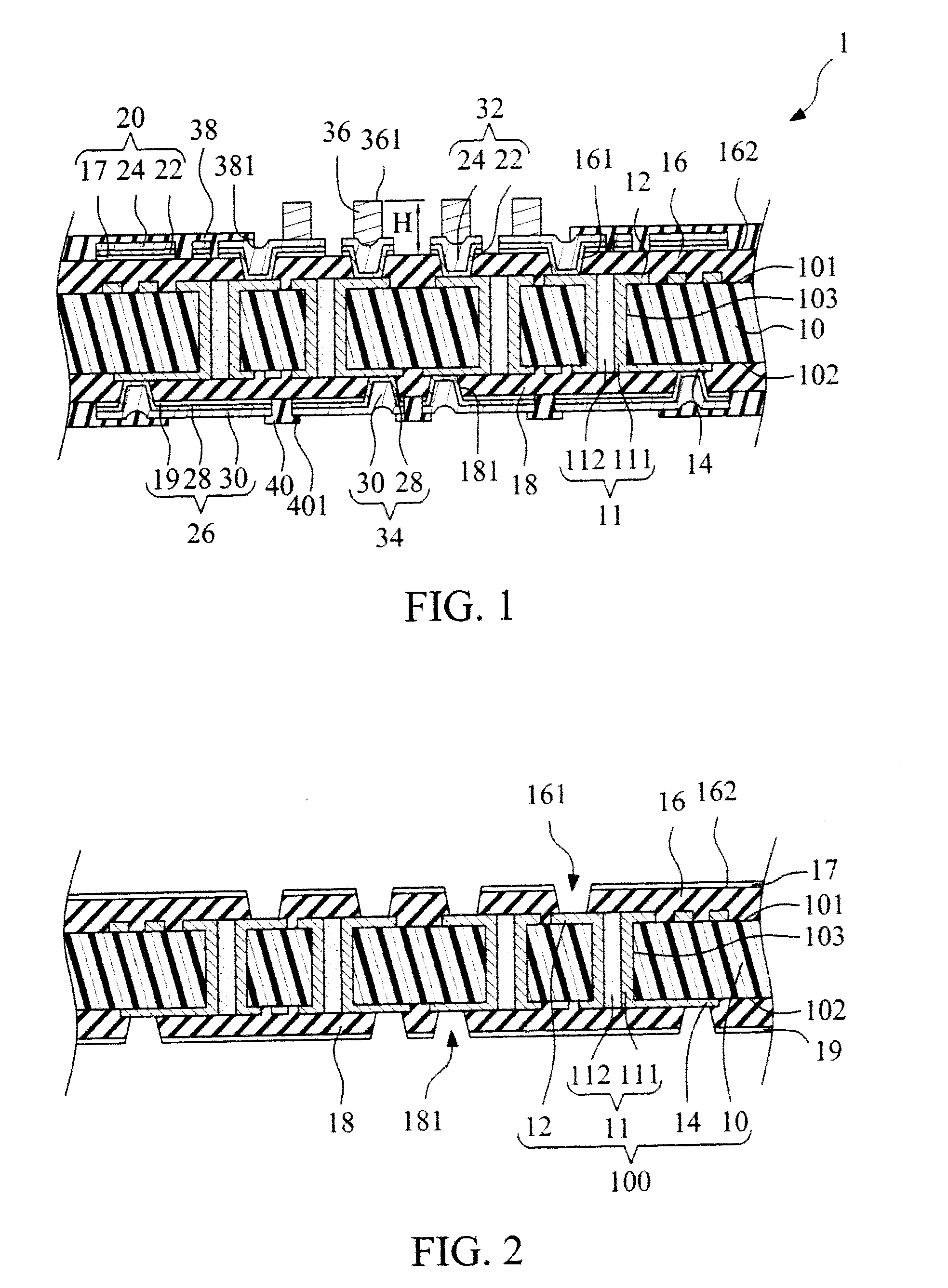
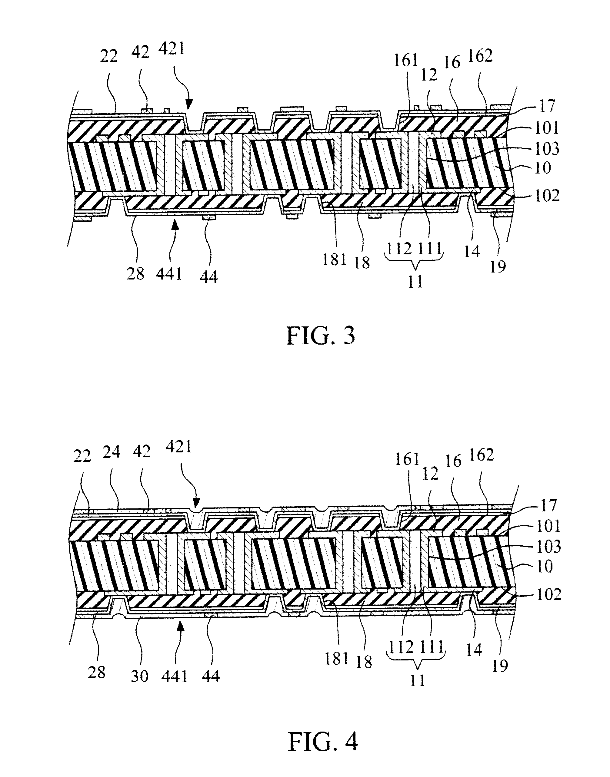
[0034]Referring to FIG. 1, a package substrate according to one of the present embodiments is illustrated. The package substrate 1 comprises a core portion 10, a plurality of conductive vias 11, an upper inner circuit layer 12, a lower inner circuit layer 14, an upper dielectric layer 16, an upper conductive foil 17, a lower dielectric layer 18, a lower conductive foil 19, an upper outermost circuit layer 20, a lower outermost circuit layer 26, a plurality of upper interconnection metals 32, a plurality of lower interconnection metals 34, a plurality of pillars 36, an upper protection layer 38, and a lower protection layer 40. Although the substrate 1 is illustrated as including four circuit layers, in other embodiments, the substrate I may include only one, two, three, or five or more circuit layers.
[0035]The core portion 10 has an upper surface 101, a lower surface 102 and a plurality of through holes 103. The core portion 10 may be made of a fiber-reinforced resin material and / or...
PUM
| Property | Measurement | Unit |
|---|---|---|
| height | aaaaa | aaaaa |
| height deviation | aaaaa | aaaaa |
| height | aaaaa | aaaaa |
Abstract
Description
Claims
Application Information
 - R&D Engineer
- R&D Manager
- IP Professional
- Industry Leading Data Capabilities
- Powerful AI technology
- Patent DNA Extraction
Browse by: Latest US Patents, China's latest patents, Technical Efficacy Thesaurus, Application Domain, Technology Topic.
© 2024 PatSnap. All rights reserved.Legal|Privacy policy|Modern Slavery Act Transparency Statement|Sitemap