Hierarchical power map for low power design

a low-power integrated circuit and hierarchy technology, applied in the field of computer-implemented methods for debugging low-power integrated circuits (ic) design, can solve the problems of inefficient and error-prone designers to debug the entire chip, and the ic becomes more difficult to debug, so as to achieve quick understanding and easy debugging

Inactive Publication Date: 2014-01-09
SYNOPSYS INC
View PDF2 Cites 32 Cited by
  • Summary
  • Abstract
  • Description
  • Claims
  • Application Information

AI Technical Summary

Benefits of technology

[0011]In accordance with embodiments of the present invention, power information is displayed in a graphic window, referred to as a power map, to help users quickly understand the power structure an

Problems solved by technology

For example, as more circuits are integrated on a system-on-chip (SoC) IC to perform increasingly more complex functions at lower power, the IC becomes more difficult to debug.
Since traditional hardware description languages (HDL) are not adequate to specify the power design information

Method used


Image

  • Hierarchical power map for low power design
  • Hierarchical power map for low power design
  • Hierarchical power map for low power design

Examples


Embodiment Construction

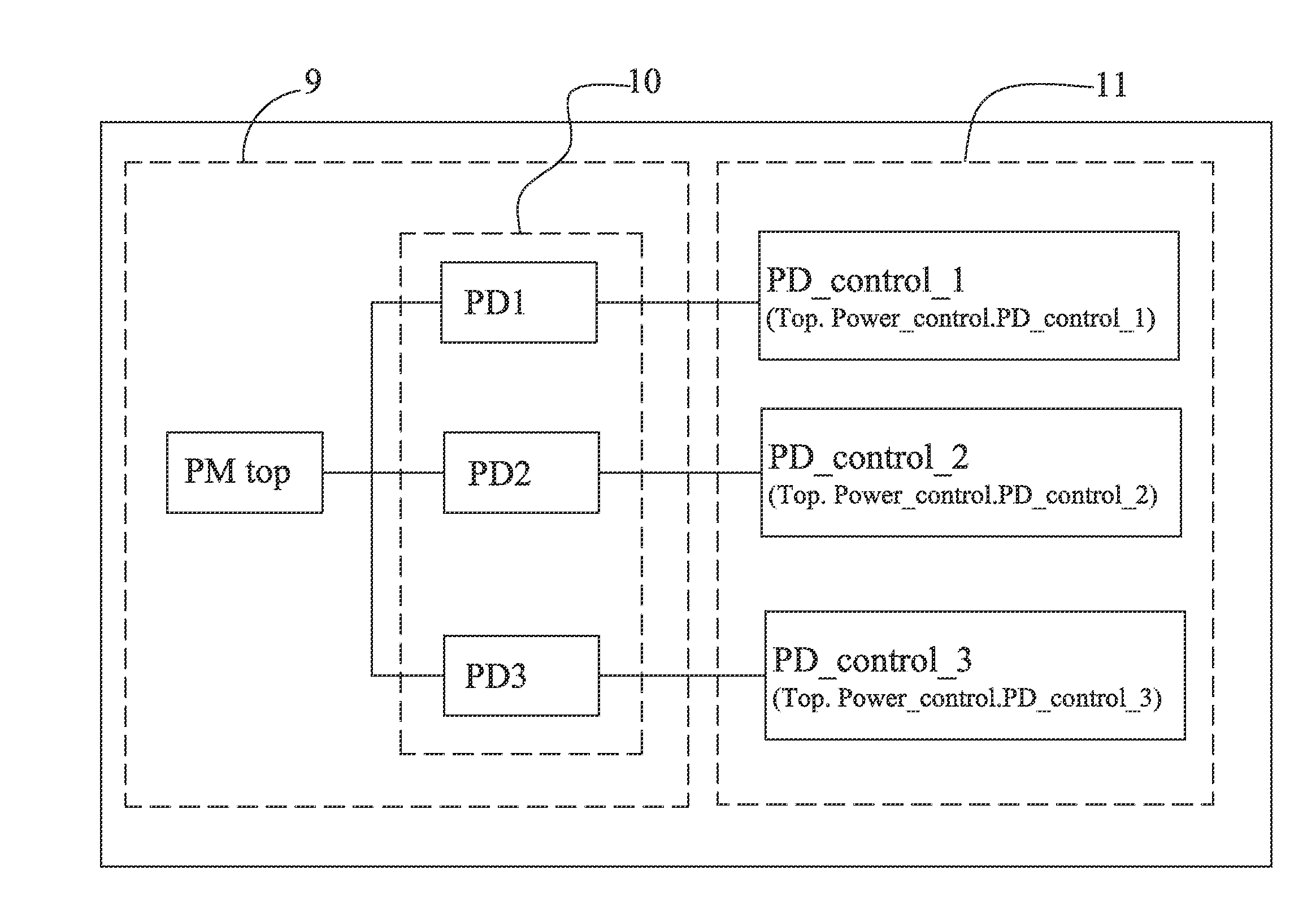
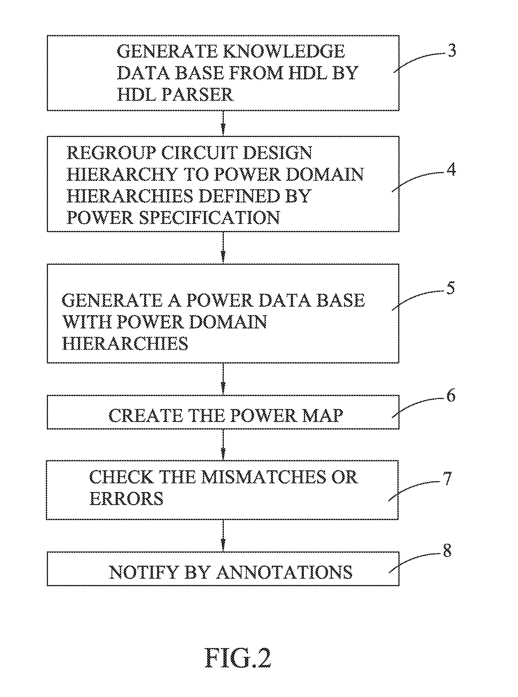
[0032]FIG. 2 is a flowchart for creating a power map of an Integrated Circuit (IC), in accordance with one embodiment of the present invention. At 3, the original text-based circuit design HDL codes are parsed and transformed into an internal structure and stored in a knowledge database. The knowledge database, which may be generated by an HDL parser, is an internal computer-readable data structure (which may have a hierarchical or a flattened structure) of the circuit design, and may be manipulated or controlled by software. At 4, power designs specified in CPF or UPF are parsed and transformed into internal structure by a CPF or UPF parser. Next, the original circuit design hierarchy in the knowledge database is regrouped into new design hierarchies defined by the power specification having a multitude of power domains. In the new hierarchies, the instances sharing the same power domain are grouped together. It is understood that the original design is not limited to hierarchical ...


PUM


Abstract

Power information associated with an IC design is displayed graphically and hierarchically using a power map, thereby providing an intuitive way for describing the power distribution among various power domains of the IC and parent-child relationships within the power domains. Each power domain is associated with a power control for controlling the power domain. The status of the power control for each power domain is displayed on the power map. The power map may include a token to set and display current operating mode of the IC design to enable the IC design to be debugged under different operating modes.

Description

CROSS-REFERENCE TO RELATED APPLICATIONS[0001]This application is a continuation-in-part of U.S. application Ser. No. 13 / 158,471, filed Jun. 13, 2011, and entitled “Hierarchical power map for low power design,” which claims the benefit of priority of U.S. Provisional Application No. 61 / 358,002, filed Jun. 24, 2010, and entitled “Method and system for displaying IC design intent with power domain intent,” the contents of which are incorporated herein by reference in their entirety.BACKGROUND OF THE INVENTION[0002]The present invention relates to a computer-implemented method for debugging low power integrated circuit (IC) design, and in particular, to a method for creating an integrated graphic user interface to debug the IC design and provide a map of its power usage.[0003]Mobile and consumer electronic devices such as personal mobile computers, MP3 audio players, notebooks and digital cameras are in wide use. The drive twoards low power consumption in increasingly thinner and lighte...

Claims


Application Information

Patent Timeline
IPC IPC(8): G06F17/50
CPCG06F17/5022G06F30/33G06F2119/06
Inventor HSU, CHIH-NENGLIN, I-LIANGFENG, WEN-CHI
Owner SYNOPSYS INC
Why Eureka
Try Eureka