Piezoelectric device

a technology of piezoelectric devices and piezoelectric plates, which is applied in piezoelectric/electrostrictive/magnetostrictive devices, piezoelectric/electrostriction/magnetostriction machines, etc., can solve the problems of difficult control of coercive electric fields, significant changes in coercive electric fields, and failure to obtain strain x in a desired direction, etc., to achieve greater compressive stress, greater compressive stress, and easy compression stress

Active Publication Date: 2014-02-06
TDK CORPARATION
View PDF12 Cites 11 Cited by
  • Summary
  • Abstract
  • Description
  • Claims
  • Application Information

AI Technical Summary

Benefits of technology

[0024]Without such substrates, there are no restraints on the piezoelectric film from the substrates and thus greater compressive stress can be exerted on the piezoelectric film.
[0025]The first and second nonmetal electroconductive intermediate films can be inorganic oxide films respectively. It is easier to make the inorganic oxide films of materials with a larger linear expansion coefficient than the piezoelectric film, and thus it is easier to exert the compressive stress on the piezoelectric film, by depositing the two inorganic oxide films at high temperature and thereafter cooling them. When the inorganic oxide films are used as the electroconductive intermediate films, it becomes feasible to deposit the electroconductive intermediate film on the piezoelectric film at high temperature or to anneal the electroconductive intermediate films, which enables greater compressive stress to be exerted on the piezoelectric film. This enables introduction of compressive stress to the piezoelectric film by heating and cooling during annealing the electroconductive intermediate films, in addition to thermal expansion of the electroconductive intermediate films, so as to enhance the effect of increase in coercive electric field.
[0026]The two inorganic oxide films can have the same composition. Furthermore, the two electroconductive intermediate films can have respective thicknesses approximately equal to each other. This configuration allows uniform compressive stresses to be exerted on the piezoelectric film from the two sides thereof.

Problems solved by technology

This means that even if the electric field E is increased in order to obtain a large strain x, the polarization direction will reverse just over the coercive electric field Ec, so as to result in failure in obtaining the strain x in a desired direction.
One of techniques to increase the coercive electric field is to change the composition of the piezoelectric film (Patent Literatures 1 and 2), but even in the case of the piezoelectric material of the same composition, when it is formed as a thin film, as described above, the coercive electric field changes significantly because of the external stress due to the film configuration of the device, the internal stress due to film forming conditions, and factors such as crystallinity and orientation of the piezoelectric film, and the control thereof is difficult.
When the coercive electric field is increased by the change in the composition of the piezoelectric film itself, the piezoelectric constants of the piezoelectric film tend to decrease, and it is thus difficult to obtain a desired displacement.
There is another technique to efficiently drive the piezoelectric film with a small coercive electric field (Patent Literature 3), but it requires preliminary measurement of accurate values of the coercive electric field, which makes a drive circuit complicated and which increases the cost of the device.

Method used


Image

  • Piezoelectric device
  • Piezoelectric device
  • Piezoelectric device

Examples


first embodiment

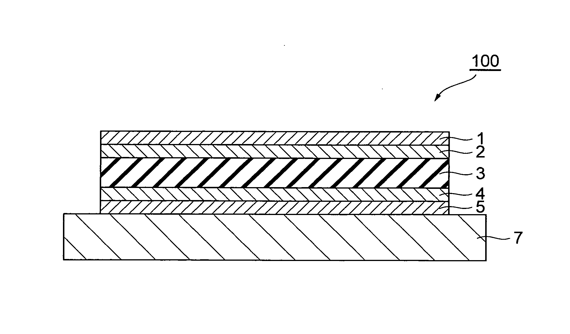
[0035]FIG. 3 shows a piezoelectric device 100 according to the first embodiment of the present invention. The piezoelectric device 100 has a substrate 7, a first electrode film 5 laid on the substrate 7, a first electroconductive intermediate film 4 laid on the first electrode film 5, a piezoelectric film 3 laid on the first electroconductive intermediate film 4, a second electroconductive intermediate film 2 formed on the piezoelectric film 3, and a second electrode film 1 formed on the second electroconductive intermediate film 2.

[0036](Substrate 7)

[0037]The substrate 7 is a plate serving as an underlying structure.

[0038]The substrate 7 to be used herein can be, for example, a silicon substrate having the (100) plane orientation. The substrate 7 can have the thickness, for example, in the range of 10 μm to 1000 μm. The substrate 7 to be used herein can also be a silicon substrate having a plane orientation different from the (100) plane, a Silicon-on-Insulator (SOI) substrate, a q...

second embodiment

[0066]A piezoelectric device 200 according to the second embodiment will be described with reference to FIG. 4. The piezoelectric device 200 of the present embodiment is different from the piezoelectric device 100 in that the substrate 7 as an underlying structure below the first electrode film 5 is removed. Because of this configuration, the top surface of the second electrode film 1 and the bottom surface of the first electrode film 2 are exposed to the outside. Since there are no restraints on expansion and compression by the substrate 7 in the piezoelectric device 200, the piezoelectric film 3 readily has much greater compressive stress. This enhances the effect of increase in coercive electric field. Since the device becomes lighter in weight by the weight of the substrate 7, the device can have a greater displacement. There are no specific restrictions on the magnitude of the compressive stress on the piezoelectric film 3, but it may be, for example, in the range of 20 to 400 ...

third embodiment

[0068]A piezoelectric device 300 according to the third embodiment will be described with reference to FIG. 5. The piezoelectric device 300 of the present embodiment is different from the piezoelectric device 100 in that the substrate 7 as an underlying structure below the first electrode film 5 is removed and in that a resin film 11 is provided on the second electrode film 1 so as to be in contact with the second electrode film 1. The films 1-5 are supported by the resin film 11 with lower rigidity, instead of the substrate 7 with high rigidity, which reduces stress exerted on the films 1-5 by the substrate 7, so as to allow greater compressive stress to be introduced to the piezoelectric film 3 from the first and second electroconductive intermediate films 2, 4, thereby enhancing the effect of increase in coercive electric field. Furthermore, the piezoelectric film 3 becomes less likely to be hindered from displacement by the substrate 7, which results in achieving more adequate d...


PUM


Abstract

A piezoelectric device according to the present invention is provided with a first electrode film, a first nonmetal electroconductive intermediate film provided on the first electrode film, a piezoelectric film provided on the first nonmetal electroconductive intermediate film, a second nonmetal electroconductive intermediate film provided on the piezoelectric film, and a second electrode film provided on the second nonmetal electroconductive intermediate film. A linear expansion coefficient of the first nonmetal electroconductive intermediate film is larger than those of the first electrode film and the piezoelectric film, and a linear expansion coefficient of the second nonmetal electroconductive intermediate film is larger than those of the second electrode film and the piezoelectric film.

Description

BACKGROUND OF THE INVENTION[0001]1. Field of the Invention[0002]The present invention relates to a piezoelectric device using a piezoelectric material.[0003]2. Related Background Art[0004]Recently, practical application of piezoelectric devices using thin film piezoelectric materials is spreading, in place of bulk piezoelectric materials. Examples of such application include gyro sensors, shock sensors, microphones, etc. making use of the piezoelectric effect to convert a force exerted on a piezoelectric film to a voltage, or actuators, ink jet heads, speakers, buzzers, resonators, etc. making use of the inverse piezoelectric effect to deform a piezoelectric film with application of voltage thereto.[0005]Reduction in thickness of the piezoelectric material will enable reduction in scale of the piezoelectric device to expand fields of application. Since a large number of piezoelectric devices can be manufactured together on a substrate, mass productivity must increase. Furthermore, t...

Claims


Application Information

Patent Timeline
Patent Type & Authority Applications(United States)
IPC IPC(8): H01L41/047
CPCB41J2/14233H10N30/878H10N30/10516H10N30/8542H10N30/073H10N30/076H10N30/877
Inventor KURACHI, KATSUYUKIAIDA, YASUHIROSAKUMA, HITOSHIMAEJIMA, KAZUHIKO
Owner TDK CORPARATION
Why Eureka
Try Eureka