Organic electroluminescent diode device, display panel, and manufacturing method thereof

a technology of electroluminescent diodes and display panels, which is applied in the direction of semiconductor devices, basic electric elements, electrical appliances, etc., can solve the problems of severe voltage drop of panels, short operating life of panels, uneven brightness of panels, etc., and achieve the effect of increasing the effect of electron injection and reducing the potential gap

Active Publication Date: 2021-10-28
SHENZHEN CHINA STAR OPTOELECTRONICS SEMICON DISPLAY TECH CO LTD
View PDF0 Cites 0 Cited by
  • Summary
  • Abstract
  • Description
  • Claims
  • Application Information

AI Technical Summary

Benefits of technology

[0017]An advantage of the present invention is that an organic electroluminescent diode device and a display panel of the present invention can effectively reduce a potential gap between the first electrode layer and the electron injection layer by adding a conductive layer between a first electrode layer and an electron injection layer of the organic electroluminescent diode device, thereby increasing an effect of electron injection. In addition, the organic light-emitting diode device in the present invention is an inverted OLED device, which is not impacted by the degraded characteristics of the OLED, so that the display panel does not have the problem of image sticking, and can thereby solve the problem of uneven brightness caused by the IR drop of the panel.

Problems solved by technology

However, there are still many problems with the currently developed top-emitting IJP OLED structure.
One of the most critical issues of the top-emitting IJP OLED structure is that a top electrode is implemented with a thinner cathode material, which usually has a larger resistance, so when conducting current, the panel has a severe voltage drop (IR drop), wherein the larger a size of a panel, the more obvious the IR drop, and since a terminal input voltage is a fixed value, an in-plane voltage will be uneven, resulting in uneven brightness of the panel.
However, how to improve the structure of the OLED device more effectively to eliminate impact of IR drop is a major problem for an OLED panel manufacturer at present.
Meanwhile, due to degradation of the device itself, the IJP OLED structure has a high operating current density when the panel is lit, resulting in a short operating life of the panel.
In addition, because the device is degraded, under the same brightness, the operating current must be increased with the time of use, which causes a source voltage of a thin film transistor to increase significantly, resulting in image sticking of the panel.
Therefore, how to solve the problem of image sticking is another difficult problem for various OLED device manufacturers.

Method used


Image

  • Organic electroluminescent diode device, display panel, and manufacturing method thereof

Examples


Embodiment Construction

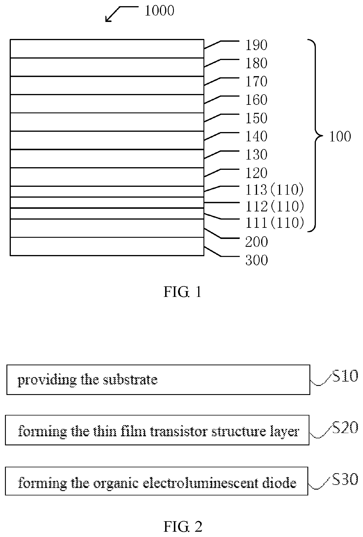
[0031]The preferred embodiments of the present invention are described below with reference to the accompanying drawings, which are configured to exemplify the embodiments of the present invention, which can fully describe the technical contents of the present invention to make the technical content of the present invention clearer and easy to understand. However, the present invention may be embodied in many different forms of embodiments, and the scope of the present invention is not limited to the embodiments set forth herein.

[0032]In the drawings, the spatially relative terms are intended to encompass different orientations in addition to the orientation as depicted in the figures. Moreover, the size and thickness of each component shown in the drawings are arbitrarily shown for ease of understanding and description, and the invention does not limit the size and thickness of each component. In order to make the illustration clearer, the thickness of components is exaggerated in ...


PUM

PropertyMeasurementUnit
thicknessaaaaaaaaaa
thicknessaaaaaaaaaa
thicknessaaaaaaaaaa

Abstract

The present invention provides an organic electroluminescent diode device, a display panel, and a manufacturing method thereof. The organic electroluminescent diode device includes a first electrode layer, a conductive layer, an electron injection layer, a light-emitting layer, a hole injection layer, and a second electrode layer, and the conductive layer is provided between the first electrode layer and the electron injection layer.

Description

BACKGROUND OF INVENTIONField of Invention[0001]The invention relates to a field of display devices, in particular to an organic electroluminescent diode device, a display panel, and a manufacturing method thereof.Description of Prior Art[0002]Ink-jet printing an organic light-emitting diode (IJP OLED) is a novel type of display technology, which has physical advantages unmatched by liquid crystal display (LCD) technology, and possesses characteristics such as active light emission, high color reality, infinite contrast, zero delay, transparent display, flexible display, free display form, and so on, and thus is the display technology of next generation that can replace the liquid crystal display technology. The IJP OLED display technology has a structure simpler than LCD since it does not require support by backlight, such that the display product can be made lighter and thinner. Moreover, its working conditions have a series of advantages such as low driving voltage, low energy con...

Claims


Application Information

Patent Timeline
Patent Type & Authority Applications(United States)
IPC IPC(8): H01L51/52H01L51/56
CPCH01L51/5231H01L27/3244H01L51/56H10K59/12H10K50/824H10K2102/321H10K59/1201H10K71/00H10K50/818H10K50/826H10K2102/3026H10K50/82H10K59/123
Inventor YUAN, WEI
Owner SHENZHEN CHINA STAR OPTOELECTRONICS SEMICON DISPLAY TECH CO LTD
Why Eureka
Try Eureka