Semiconductor buffer structure, semiconductor device including the same, and manufacturing method thereof

a semiconductor device and buffer structure technology, applied in the direction of semiconductor devices, basic electric elements, electrical equipment, etc., can solve the problems of substrate warpage at high temperatures, high cost of silicon substrates, and difficult processing, and achieve the effect of increasing the compression stress

Active Publication Date: 2014-03-06
SAMSUNG ELECTRONICS CO LTD
View PDF10 Cites 1 Cited by
  • Summary
  • Abstract
  • Description
  • Claims
  • Application Information

AI Technical Summary

Benefits of technology

[0030]The at least one property of the fourth layer may allow the second nitride semiconductor layer to have greater compression stress than tensile stress.
[0031]The at least one property of the fourth layer allows the structure to have a net compressive stress.
[0032]In accordance with another embodiment, a method of manufacturing a semiconductor buffer structure, the method including: forming a first nitride semiconductor layer on a silicon substrate; forming a dislocation control layer made from Ala1Inb1Ga1-a1-b1N (0≦a1, b1≦1, a1+b1≠1) on the first nitride semiconductor layer; and formforming a second nitride semiconductor layer on the dislocation control layer, wherein an average gallium composition ratio of each of the first and second nitride semiconductor layers increases in one direction, the average gallium composition ratio of the second nitride semiconductor layer is higher than the average gallium composition ratio of the first nitride semiconductor layer, and the dislocation control layer reduces the overall dislocation density of the first and second nitride semiconductor layers.

Problems solved by technology

Many nitride-based semiconductor devices use sapphire substrates that are expensive, hard to process, and have low electric conductivity.
Also, when a sapphire substrate is epitaxially grown to a large size, the substrate may warp at high temperatures due to a low thermal conductivity.
Consequently, it is difficult to make sapphire substrates large in size.
However, the approach of using silicon substrates in nitride-based devices is not without drawbacks.
For example, when a nitride buffer structure is grown on a silicon substrate, dislocation density may increase due to a mismatch in a gallium composition ratio between the substrate and the nitride buffer structure.
This mismatch may promote the formation of cracks, which can compromise proper operation of the device or, in a worst case, render the device inoperative.

Method used


Image

  • Semiconductor buffer structure, semiconductor device including the same, and manufacturing method thereof
  • Semiconductor buffer structure, semiconductor device including the same, and manufacturing method thereof
  • Semiconductor buffer structure, semiconductor device including the same, and manufacturing method thereof

Examples


Embodiment Construction

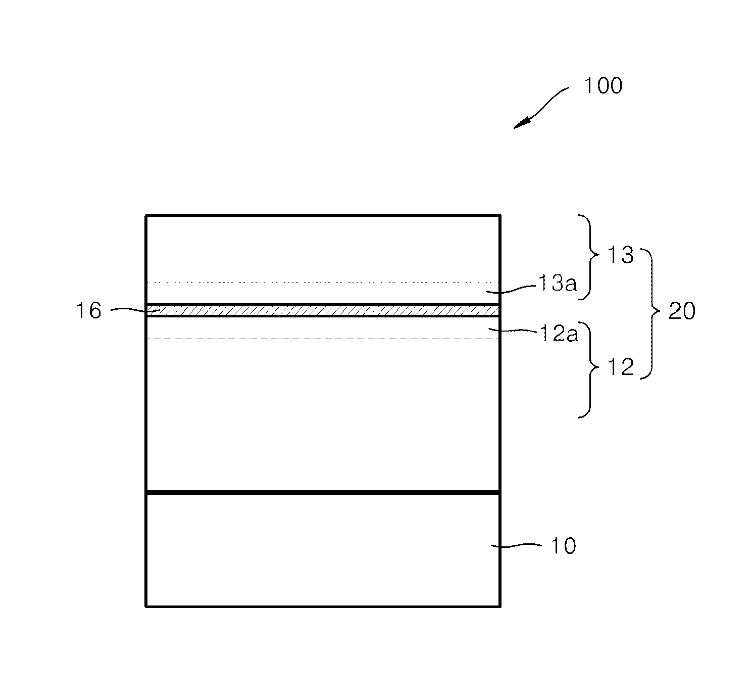
[0047]The present invention will now be described more fully with reference to the accompanying drawings, in which exemplary embodiments of the invention are shown. The invention may, however, be embodied in many different forms and should not be construed as being limited to the embodiments set forth herein. Rather, these embodiments are provided so that this disclosure will be thorough and complete, and will fully convey the concept of the invention to those of ordinary skill in the art.

[0048]In the drawings, it is understood that the thicknesses of layers and regions may be exaggerated for clarity. It will also be understood that when a layer is referred to as being “on” another layer or substrate, it can be directly on the other layer or substrate or intervening layers may also be present. Like reference numerals in the drawings denote like elements, and thus their description will not be repeated. As used herein, the term “and / or” includes any and all combinations of one or mor...


PUM

PropertyMeasurementUnit
thicknessaaaaaaaaaa
thicknessaaaaaaaaaa
thicknessaaaaaaaaaa

Abstract

A semiconductor structure including a first nitride semiconductor layer, a second nitride semiconductor layer, and a third layer between the first nitride semiconductor layer and the second nitride semiconductor layer. The first nitride semiconductor layer has a first gallium composition ratio, the second nitride semiconductor layer has a second gallium composition ratio different from the first metal composition ratio, and the third layer has a third gallium composition ratio greater than at least one of the first gallium composition ratio or the second gallium composition ratio. The structure may also include a fourth layer for reducing tensile stress or increasing compression stress experienced by at least the second nitride semiconductor layer.

Description

CROSS-REFERENCE TO RELATED APPLICATIONS[0001]This application claims the benefit of Korean Patent Application No. 10-2012-0097863, filed on Sep. 4, 2012, in the Korean Intellectual Property Office, the disclosure of which is incorporated herein in its entirety by reference.BACKGROUND[0002]1. Field[0003]One or more embodiments herein relate to a semiconductor buffer structure, a semiconductor device including the semiconductor buffer structure, and a method of manufacturing the semiconductor buffer structure and the semiconductor device.[0004]2. Description of the Related Art[0005]Many nitride-based semiconductor devices use sapphire substrates that are expensive, hard to process, and have low electric conductivity. Also, when a sapphire substrate is epitaxially grown to a large size, the substrate may warp at high temperatures due to a low thermal conductivity. Consequently, it is difficult to make sapphire substrates large in size.[0006]Semiconductor devices which use silicon subst...

Claims


Application Information

Patent Timeline
Patent Type & Authority Applications(United States)
IPC IPC(8): H01L29/20H01L21/02
CPCH01L21/0254H01L29/2003H01L21/02381H01L21/02458H01L21/02505H01L21/0251H01L29/267H01L21/02507
Inventor KIM, JUN-YOUNKIM, JOO-SUNGYANG, MOON-SEUNG
Owner SAMSUNG ELECTRONICS CO LTD
Why Eureka
Try Eureka