Interposer for optical module, optical module using the same, method for manufacturing the same
- Summary
- Abstract
- Description
- Claims
- Application Information
AI Technical Summary
Benefits of technology
Problems solved by technology
Method used
Image
Examples
Embodiment Construction
[0024]Hereinafter, the structure and the operation according to the disclosure will be described in detail with reference to accompanying drawings. In the following description based on the accompanying drawings, the same elements will be assigned with the same reference numerals regardless of drawing numbers, and the repetition in the description of the same elements having the same reference numerals will be omitted in order to avoid redundancy. Although the terms “first” and “second” may be used in the description of various elements, the disclosure is not limited thereto. The terms “first” and “second” are used to distinguish one element from the other elements.
[0025]1. Embodiment of Manufacturing Process of Interposer for Optical Module
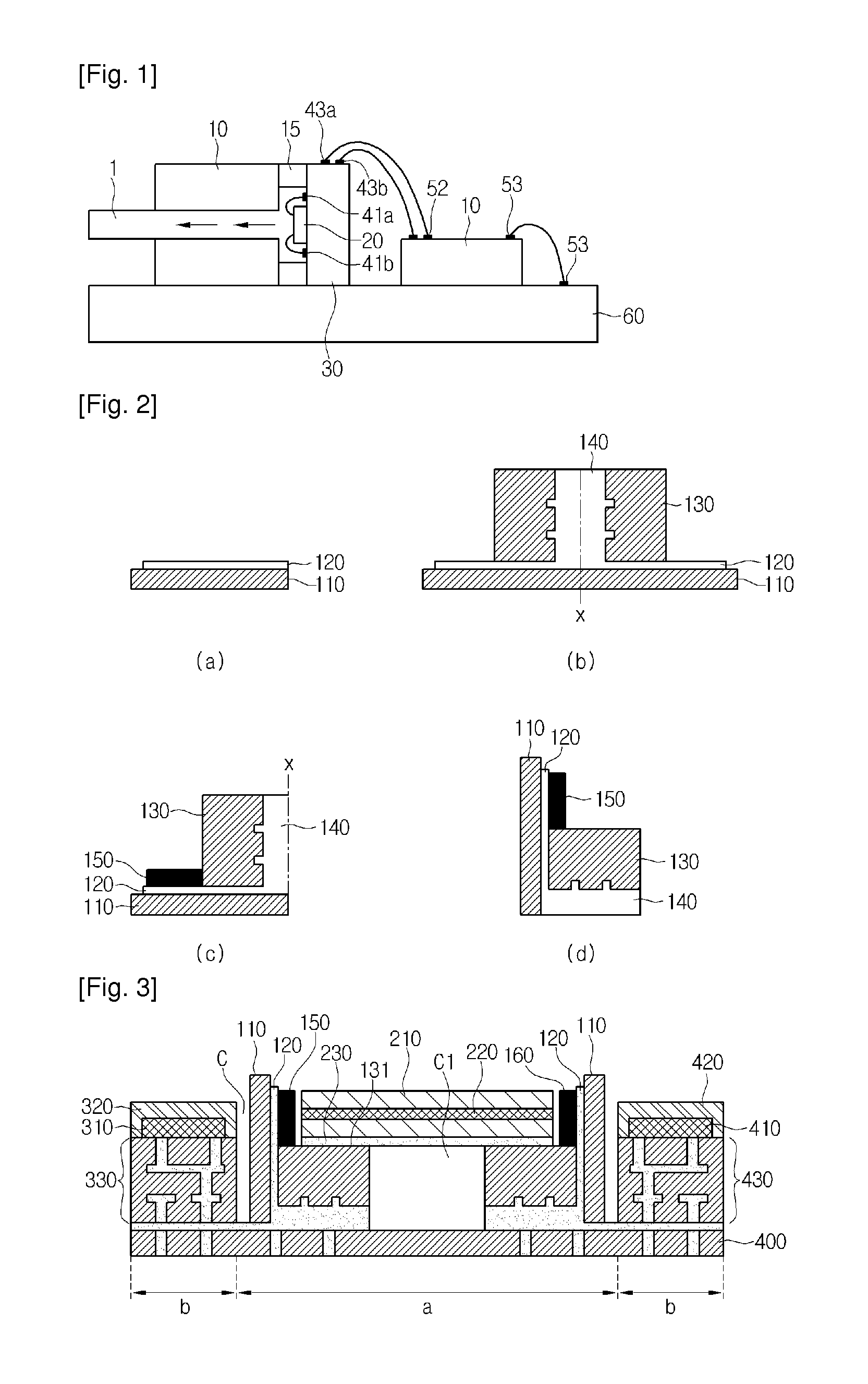
[0026]FIG. 2 illustrates views showing the manufacturing process of an interposer for an optical module according to the disclosure.
[0027]As shown in FIG. 2(a), after forming a metallic layer 120 on a first substrate 110 having an insulating prop...
PUM
| Property | Measurement | Unit |
|---|---|---|
| Angle | aaaaa | aaaaa |
| Flexibility | aaaaa | aaaaa |
| Electrical conductor | aaaaa | aaaaa |
Abstract
Description
Claims
Application Information


