Flat Panel Display and Method of Manufacturing the Same

Active Publication Date: 2014-02-20
SAMSUNG DISPLAY CO LTD
View PDF2 Cites 2 Cited by
  • Summary
  • Abstract
  • Description
  • Claims
  • Application Information

AI Technical Summary

Benefits of technology

[0010]According to an embodiment of the present invention, the gate electrode of the TFT is extended to the top of the adjacent wiring line so that capacitance is formed by the gate electrode and the wiring line that overlap each other. When the capacitance is formed between the TFT and the wiring line adjacent to the TFT,

Problems solved by technology

Since the distances among the TFTs, the capacitors, and the wiring lines are reduced as the resolution of the FPD increases, problems are generated.
Since the pa

Method used


Image

  • Flat Panel Display and Method of Manufacturing the Same
  • Flat Panel Display and Method of Manufacturing the Same
  • Flat Panel Display and Method of Manufacturing the Same

Examples


Embodiment Construction

[0020]Hereinafter, certain exemplary embodiments according to the present invention will be described with reference to the accompanying drawings. Here, when a first element is described as being coupled to a second element, the first element may be directly coupled to the second element or it may be indirectly coupled to the second element via a third element. Furthermore, some of the elements that are not essential to a complete understanding of the invention are omitted for clarity. Also, like reference numerals refer to like elements throughout.

[0021]Hereinafter, exemplary embodiments of the present invention will be described in detail with reference to the accompanying drawings. The embodiments are provided so that those skilled in the art may fully understand the present invention. Various modifications are available and the scope of the present invention is not limited to the following embodiments.

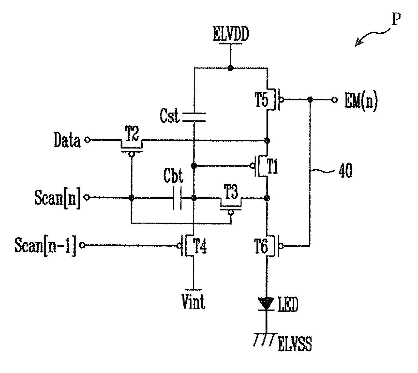
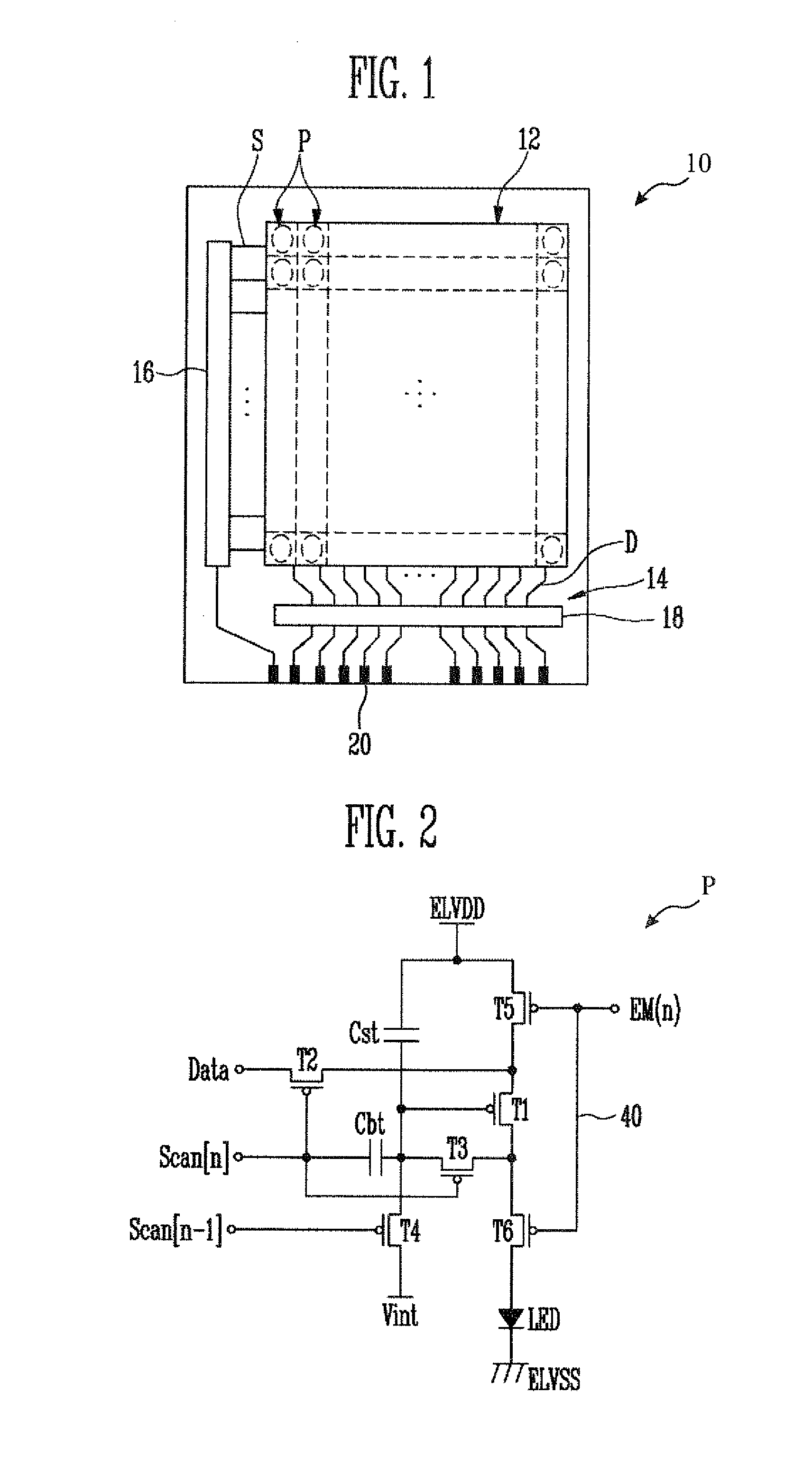
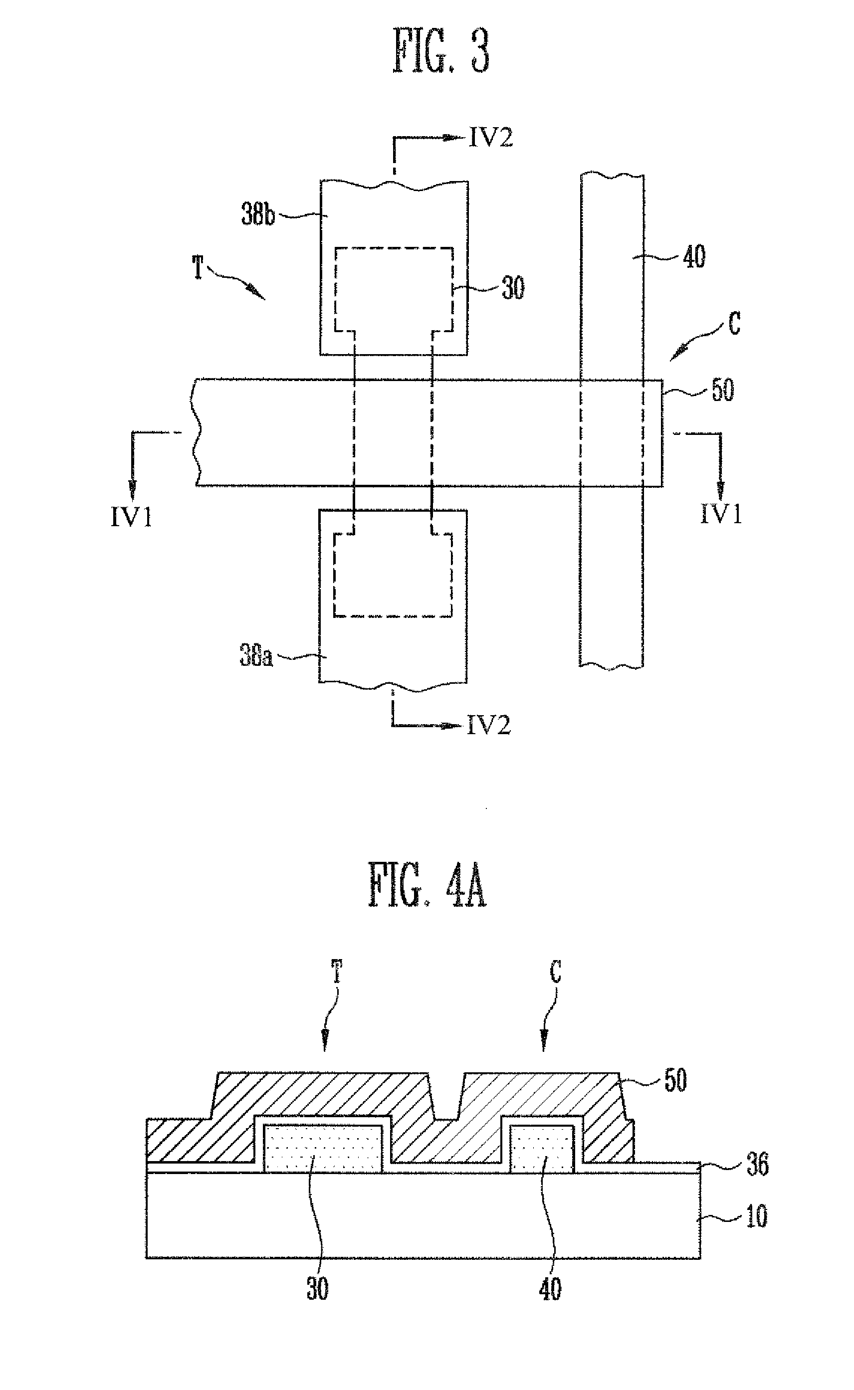
[0022]FIG. 1 is a schematic plan view illustrating a flat panel display (FPD) ...


PUM


Abstract

In a flat panel display (FPD) and a method of manufacturing the same, the FPD includes a substrate, a semiconductor layer formed on the substrate, a wiring line formed on the substrate so as to be separated from the semiconductor layer, an insulating layer formed on the semiconductor layer and the wiring line, a gate electrode formed on the insulating layer formed on the semiconductor layer and extended to a top of the wiring line, and a source electrode and a drain electrode coupled to a source region and a drain region, respectively, of the semiconductor layer. Capacitance is formed by the gate electrode and the wiring line.

Description

CLAIM OF PRIORITY[0001]This application makes reference to, incorporates the same herein, and claims all benefits accruing under 35 U.S.C. §119 from an application earlier filed in the Korean Intellectual Property Office on the 20th of August 20 and there duly assigned Serial No. 10-2012-0090751.BACKGROUND OF THE INVENTION[0002]1. Field of the Invention[0003]The present invention relates to a flat panel display and a method of manufacturing the same, and more particularly, to a flat panel display capable of preventing picture quality from deteriorating due to parasitic capacitance between thin film transistors (TFTs) and wiring lines for transmitting signals.[0004]2. Description of the Related Art[0005]A flat panel display (FPD) such as a liquid crystal display (LCD) and an organic light emitting display (OLED) includes thin film transistors (TFTs) for transmitting signals in order to drive pixels and capacitors for maintaining the signals. The TFTs and the capacitors are electrical...

Claims


Application Information

Patent Timeline
IPC IPC(8): H01L29/786H01L33/08
CPCH01L33/08H01L29/786H01L27/124G02F1/136213H01L27/1255
Inventor KIM, JONG-SEOK
Owner SAMSUNG DISPLAY CO LTD
Why Eureka
Try Eureka