Method of stress relief in Anti-reflective coated cap wafers for wafer level packaged infrared focal plane arrays

a technology of infrared focal plane array and coated cap, which is applied in the direction of synthetic resin layered products, coatings, chemistry apparatus and processes, etc., to achieve the effect of reducing the induced wafer bow

Active Publication Date: 2014-02-27
RAYTHEON CO
View PDF5 Cites 5 Cited by
  • Summary
  • Abstract
  • Description
  • Claims
  • Application Information

AI Technical Summary

Benefits of technology

[0005]In accordance with one or more embodiments, a method of reducing wafer bow induced by an anti-reflective coating on a cap wafer is provided. The method comprises providing the cap wafer having a planar side and an opposing cavity side, the cavity side including at least one recessed region and a dividing region on either side of the at least one recessed region, positioning a first shadow mask having at least one opening therein over the planar side of the cap wafer, aligning the first shadow mask such that the at least one opening is positioned opposite the at least one recessed region, and depositing at least one layer of an anti-reflective coating material through the first shadow mask onto the planar side of the cap wafer to provide a discontinuous coating on the planar side.

Problems solved by technology

Likewise, the types of MEMS devices can vary from relatively simple structures lacking any moving elements, to extremely complex electromechanical systems with multiple moving elements that are under the control of integrated microelectronics.
The vacuum package provides an optimal environment for the sensing device, since the presence of gas may impede performance.

Method used


Image

  • Method of stress relief in Anti-reflective coated cap wafers for wafer level packaged infrared focal plane arrays
  • Method of stress relief in Anti-reflective coated cap wafers for wafer level packaged infrared focal plane arrays
  • Method of stress relief in Anti-reflective coated cap wafers for wafer level packaged infrared focal plane arrays

Examples


Embodiment Construction

[0020]Aspects and embodiments are directed toward providing a method for reducing wafer bow induced by an anti-reflective coating. In particular, aspects and embodiments are directed to reducing wafer bow in a cap wafer.

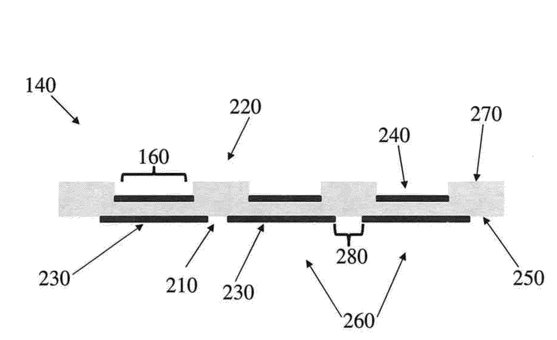
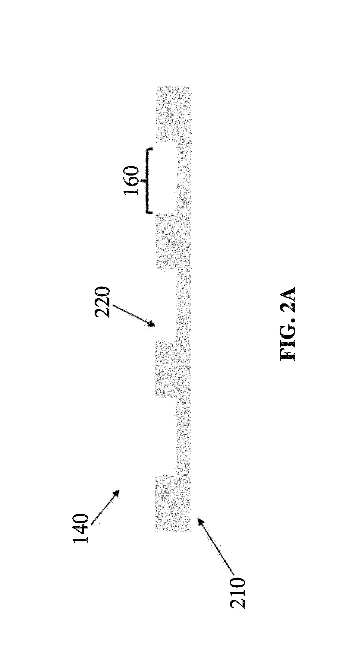
[0021]As discussed above, MEMS devices, including microbolometers, are often placed in vacuum packages to provide an isolated environment for the device. For example, a cap wafer may be bonded to an ROTC device wafer, enclosing the sensor device (for example, one or more microbolometers) to provide a protected and sealed environment surrounding the sensor device. Fabrication of the cap wafer may include coating the cap wafer with an anti-reflective (AR) coating. In certain applications, the AR coating may be included on both sides of the cap wafer. As discussed further below, the AR coating may be dimensioned differently on both sides of the wafer, which may induce internal stress in the cap wafer. The internal stress causes the cap wafer to bow or curve, which leads...


PUM

PropertyMeasurementUnit
diameteraaaaaaaaaa
diameteraaaaaaaaaa
thicknessaaaaaaaaaa

Abstract

Methods for reducing wafer bow induced by an anti-reflective coating of a cap wafer are provided. The method may utilize a shadow mask having at least one opening therein that is positioned opposite recessed regions in a cap wafer. The method may further include depositing at least one layer of an anti-reflective coating material through the shadow mask onto a planar side of a cap wafer to provide a discontinuous coating on the planar side.

Description

BACKGROUND[0001]Microelectromechanical systems (MEMS) is a technology that can generally be described as miniaturized mechanical and electro-mechanical elements that are made using the techniques of microfabrication. The critical physical dimensions of MEMS devices can vary from well below one micrometer (micron) to several millimeters. Likewise, the types of MEMS devices can vary from relatively simple structures lacking any moving elements, to extremely complex electromechanical systems with multiple moving elements that are under the control of integrated microelectronics. Non-limiting examples of MEMS devices include sensors and optical devices, such as single-band or multi-band detector focal plane arrays (FPAs) or microbolometers. FPA devices may include single-band or multi-band integrated FPAs (e.g., single band visible FPA devices, or integrated dual-band FPA devices that are capable of detecting both near infrared (IR) spectrum radiation and visible spectrum radiation).[00...

Claims


Application Information

Patent Timeline
Patent Type & Authority Applications(United States)
IPC IPC(8): B05D5/06
CPCB05D5/061B81B7/0067B81B2201/0207B81C2203/0118B81C1/00325
Inventor GOOCH, ROLAND W.DIEP, BUU Q.BLACK, STEPHEN H.KOCIAN, THOMAS A.KENNEDY, ADAM M.
Owner RAYTHEON CO
Why Eureka
Try Eureka