
Board assemblies with minimized warpage and systems and methods for making the same
a technology of assembly and warpage, applied in the direction of manufacturing tools, electrical apparatus construction details, rod connections, etc., can solve the problems of warpage, warpage, warpage, etc., and achieve the effect of reducing warpage and reducing the number o
- Summary
- Abstract
- Description
- Claims
- Application Information
AI Technical Summary
Benefits of technology
Problems solved by technology
Method used
Image

Examples
Embodiment Construction
[0029]Board assemblies having minimized warpage and systems and methods for making the same are provided and described with reference to FIGS. 1-21.
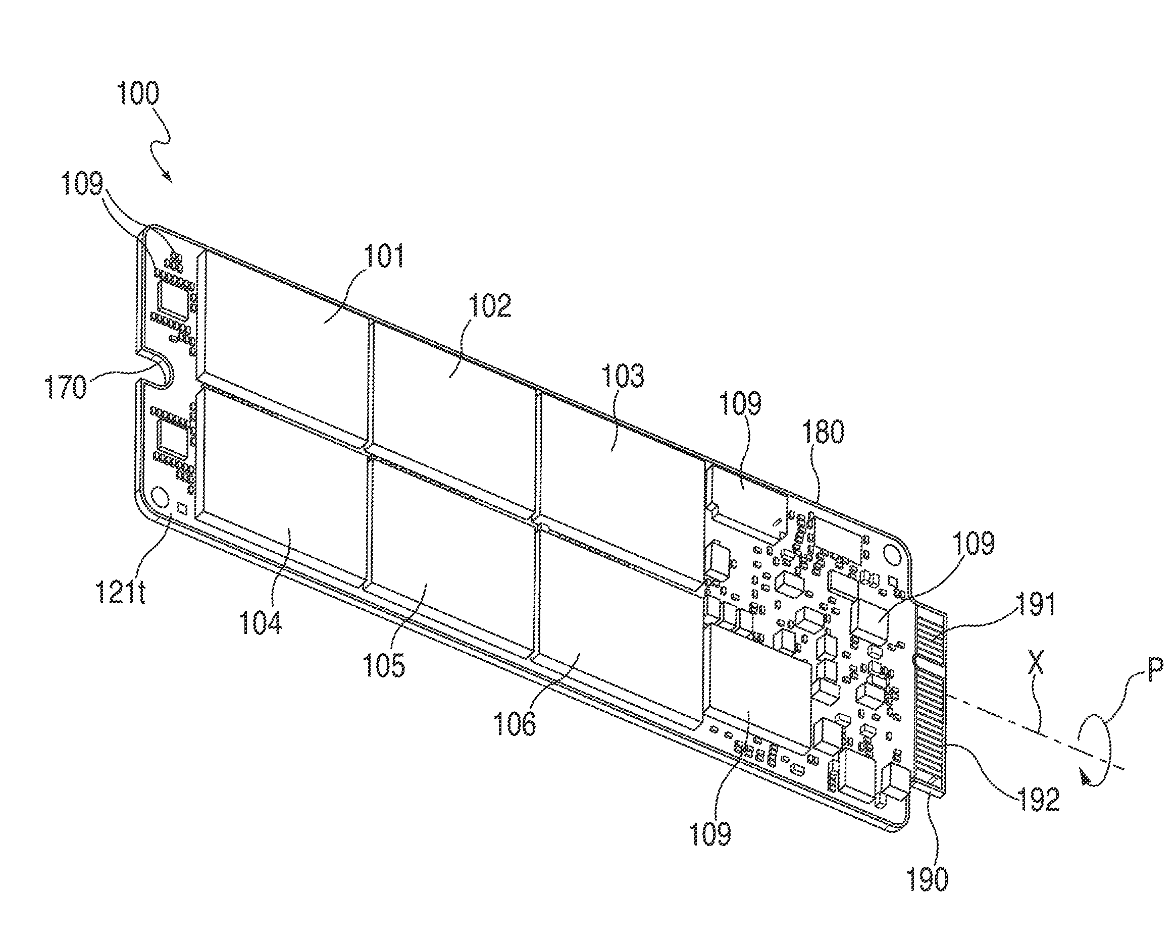
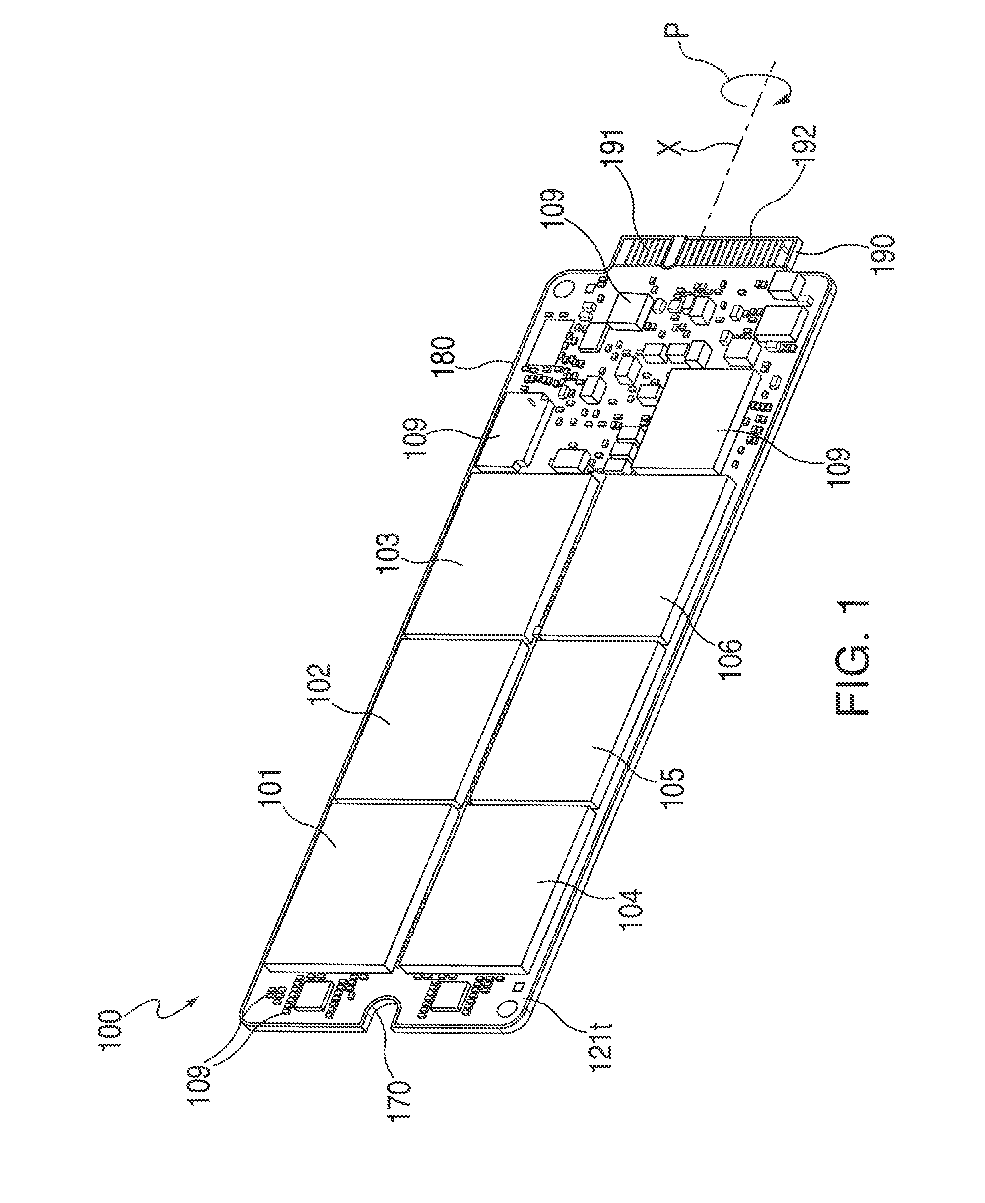
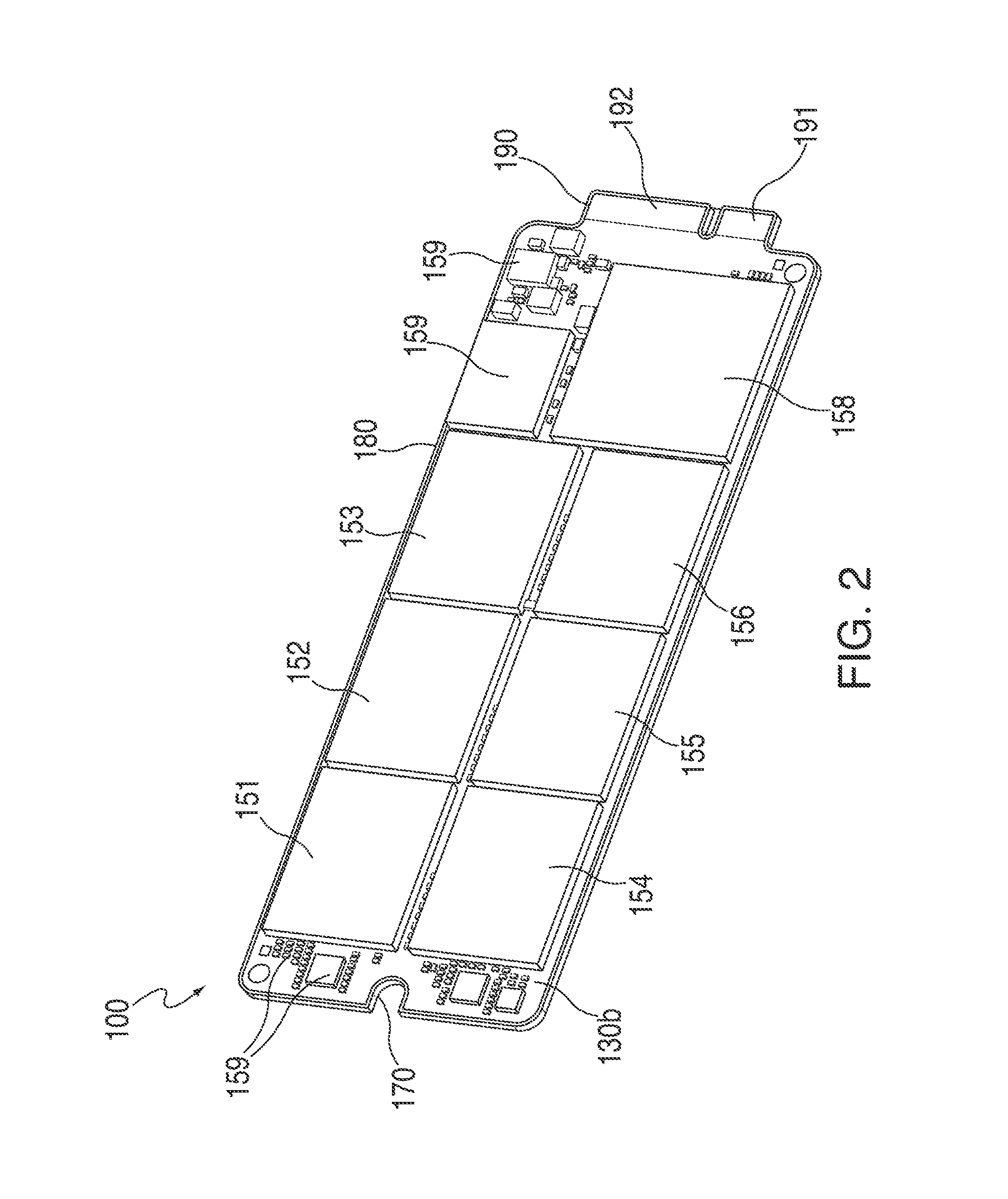
[0030]FIG. 1 shows a perspective view of a top side board, in accordance with at least one embodiment. Board 100 may be included as part of an electronic device such as, for example, a portable media player, a smart phone, a laptop computer, or a tablet. Board 100 may be configured as an SSD board which typically includes one or more arrays of NAND-flash based memory (NAND chips). NAND chips may provide higher reliability and lower power consumption than hard disk drives.
[0031]Board 100 may include a substrate 180 having one or more components mounted thereon. Substrate 180 may be composed of silicon and / or any other suitable type of material. Substrate 180 may include a plurality of layers (described later) and may include a top surface 121t. Board 100 may include NAND chips 101, 102, 103, 104, 105, and 106 that may be mounted on top su...
PUM
| Property | Measurement | Unit |
|---|---|---|
| angle | aaaaa | aaaaa |
| degree of warpage | aaaaa | aaaaa |
| threshold degree | aaaaa | aaaaa |
Abstract
Description
Claims
Application Information