Method for handling a semiconductor wafer assembly
- Summary
- Abstract
- Description
- Claims
- Application Information
AI Technical Summary
Benefits of technology
Problems solved by technology
Method used
Image
Examples
Embodiment Construction
[0038]In reading the detailed description, the accompanying drawings may be referenced at the same time and considered as part of the detailed description.
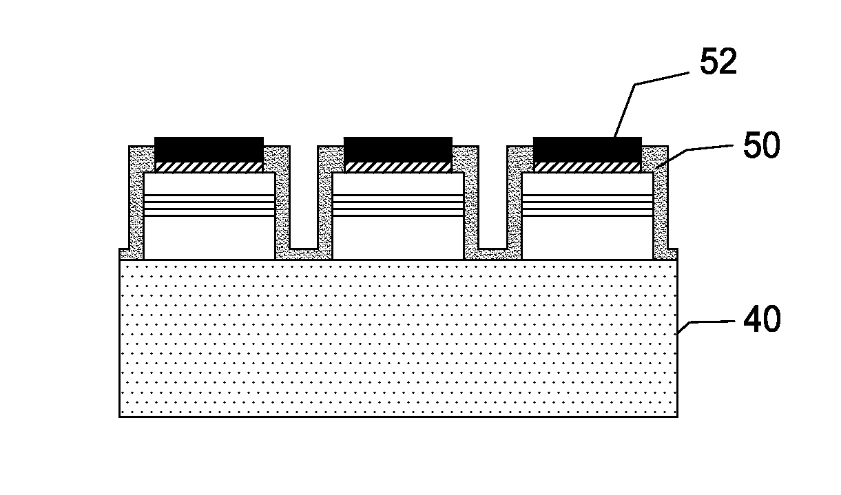
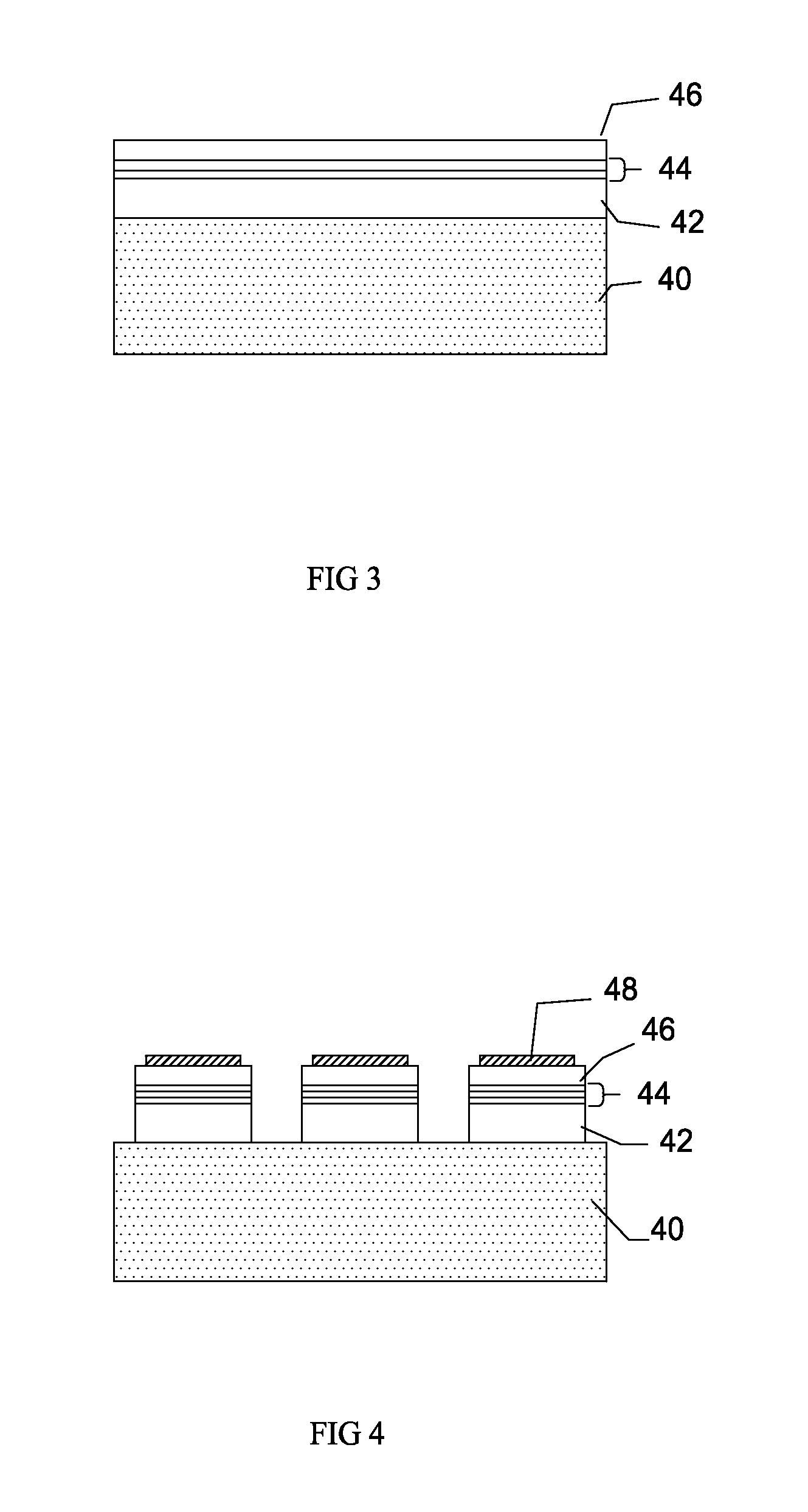
[0039]Referring to FIGS. 3 to 8, a manufacturing method for vertical LEDs is illustrated therein. In the description, the reference numerals given for the inventive device structure will be also used in the recitation of the steps of the inventive manufacturing method.
[0040]The process described below is for one embodiment with InGaN LEDs initially grown on sapphire. Electro or Electroless Chemical plating is then used to deposit a thick contact for electrical and thermal conduction for the resulting LED device. Electro or Electroless Chemical plating is used in lieu of wafer bonding. The process can be applied to any optoelectronic device where bonding was used to attach the epilayer to a new host substrate for improvement of optical, electrical and thermal properties.
[0041]For example, the techniques described herein may be appl...
PUM
 Abstract
Description
Claims
Application Information


