Encapsulating sheet-covered semiconductor element, producing method thereof, semiconductor device, and producing method thereof

Inactive Publication Date: 2014-04-03
NITTO DENKO CORP
View PDF1 Cites 9 Cited by
  • Summary
  • Abstract
  • Description
  • Claims
  • Application Information

AI Technical Summary

Benefits of technology

The present invention provides a semiconductor device that includes a plurality of semiconductor elements that are encapsulated with an encapsulating sheet. The encapsulating sheet is placed over the semiconductor elements to reduce stress and prevent shifting of position and unevenness in size. This results in a stable and reliable semiconductor device. The technical effect of this invention is to enhance the stability and reliability of semiconductor devices.

Problems solved by technology

The resin applied onto the chip, however, may be relatively hard in accordance with the purpose and use.
Then, in the chip, a shift of position (a chip shift) in which the chip is shifted from the predetermined position that is initially set in the silica glass substrate is generated and thus, a great unevenness in a size of the resin that encapsulates the chip after being subjected to dicing is generated.
As a result, there is a disadvantage that unevenness in various properties in the semiconductor device is generated.

Method used


Image

  • Encapsulating sheet-covered semiconductor element, producing method thereof, semiconductor device, and producing method thereof
  • Encapsulating sheet-covered semiconductor element, producing method thereof, semiconductor device, and producing method thereof
  • Encapsulating sheet-covered semiconductor element, producing method thereof, semiconductor device, and producing method thereof

Examples


first embodiment

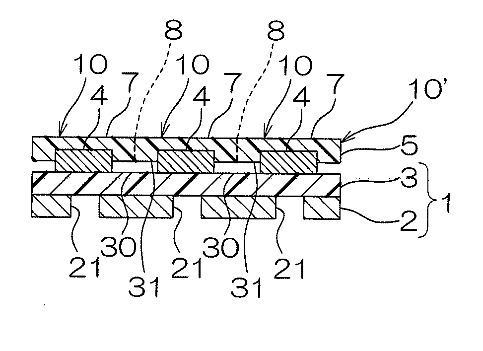
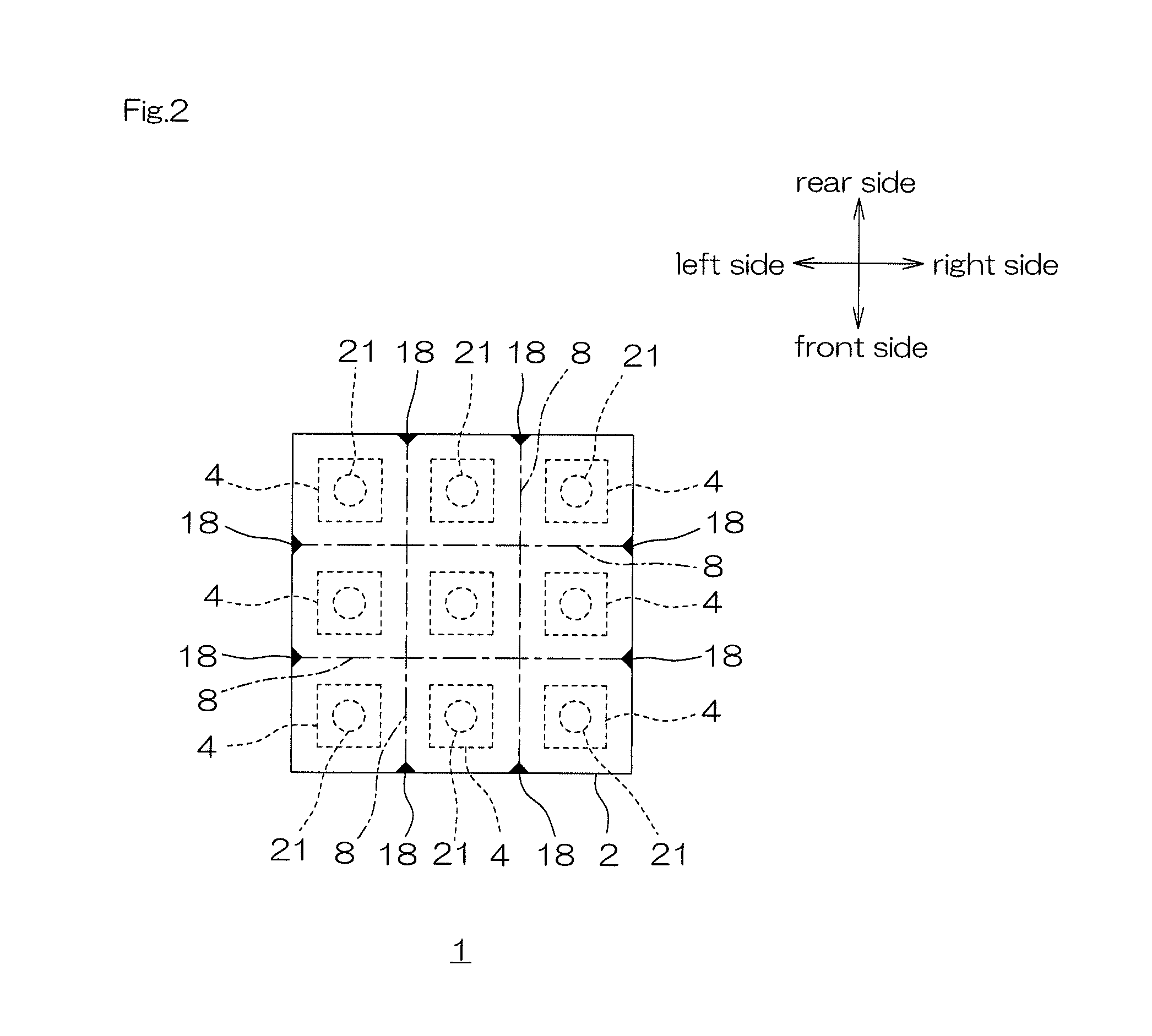
[0143]In FIG. 1, the up-down direction of the paper surface may be referred to as a first direction; the depth direction of the paper surface may be referred to as a second direction (a front-rear direction); and the right-left direction of the paper surface may be referred to as a third direction. Directions in FIG. 2 and the subsequent figures are in conformity with the directions in FIG. 1. In FIGS. 2 and 7, a pressure-sensitive adhesive layer 3 to be described later is omitted so as to clearly show the relative arrangement of a support substrate 2 and a reference mark 18 to be described later.

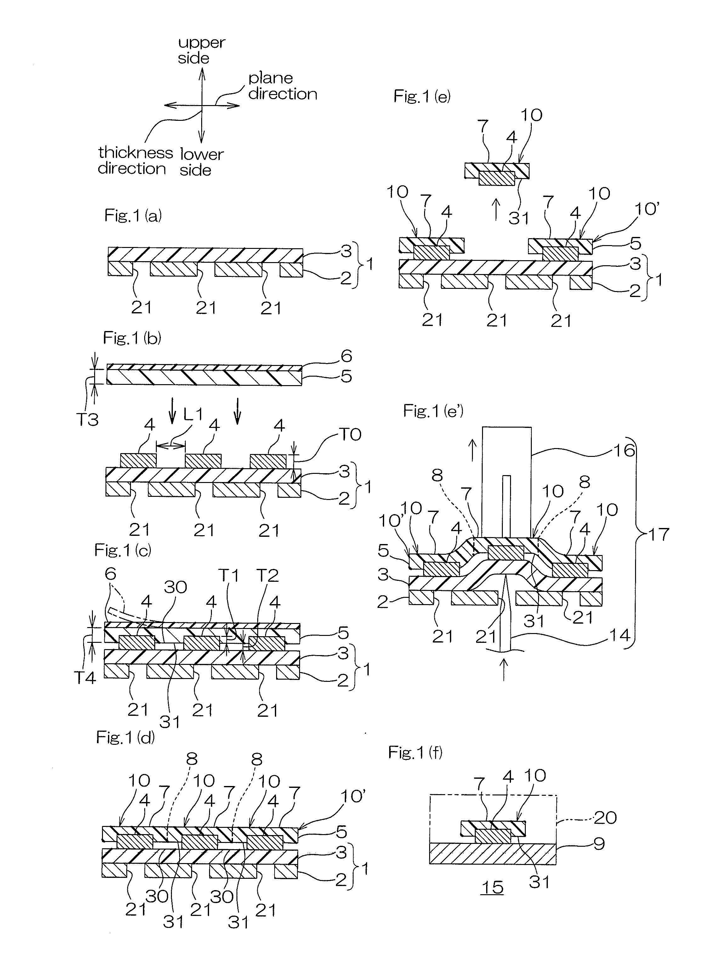
[0144]As shown in FIGS. 1 (a) to 1 (e), a method for producing a phosphor layer-covered LED 10 as an encapsulating sheet-covered semiconductor element includes a support sheet preparing step (ref: FIG. 1 (a)); an LED disposing step of disposing LEDs 4 as optical semiconductor elements that are semiconductor elements (one example of a semiconductor element disposing step, ref: FIG. 1 (b)); a...

second embodiment

[0303]In FIGS. 6 and 7, the same reference numerals are provided for members and steps corresponding to each of those in the first embodiment, and their detailed description is omitted.

[0304]In the first embodiment, the through holes 21 are provided in the support substrate 2. Alternatively, for example, as shown in FIGS. 6 (a) and 7, the support substrate 2 can be formed into a flat plate shape having no through hole 21.

[0305]As shown in FIGS. 6 (a) to 6 (e), the method for producing the phosphor layer-covered LED 10 in the second embodiment includes a support sheet preparing step of preparing the support sheet 1 (ref: FIG. 6 (a)); an LED disposing step of disposing the LEDs 4 on the support sheet 1 (ref: FIG. 6 (b)); a phosphor sheet disposing step of, after the LED disposing step, disposing the phosphor sheet 5 on the upper portions of the LEDs 4 so as to partially cover the LEDs 4 and to form the space 30 over the LEDs 4 that are adjacent to each other (ref: FIG. 6 (c)); an LED ...

third embodiment

[0341]In the views in the third embodiment, the same reference numerals are provided for members and steps corresponding to each of those in the first and second embodiments, and their detailed description is omitted.

[0342]In the LED peeling step (ref: FIG. 6 (e)) in the second embodiment, each of the phosphor layer-covered LEDs 10 is peeled from the support substrate 2 and the pressure-sensitive adhesive layer 3. Alternatively, for example, as shown in FIG. 8 (e), first, the support substrate 2 is peeled from the pressure-sensitive adhesive layer 3 and thereafter, as shown in FIG. 8 (f), each of the phosphor layer-covered LEDs 10 can be peeled from the pressure-sensitive adhesive layer 3 only.

[0343]That is, the method for producing the phosphor layer-covered LED 10 includes the same steps of support sheet preparing step (ref: FIG. 8 (a)), LED disposing step (ref: FIG. 8 (b)), phosphor sheet disposing step (ref: FIG. 8 (c)), LED encapsulating step (ref: FIG. 8 (d)), cutting step (re...


PUM


Abstract

A method for producing an encapsulating sheet-covered semiconductor element includes a semiconductor element disposing step of disposing a plurality of semiconductor elements at spaced intervals to each other and an encapsulating sheet disposing step of disposing an encapsulating sheet so as to cover a plurality of the semiconductor elements and to form a space over the semiconductor elements adjacent to each other.

Description

CROSS-REFERENCE TO RELATED APPLICATION[0001]The present application claims priority from Japanese Patent Applications No. 2012-221655 filed on Oct. 3, 2012 and No. 2013-176712 filed on Aug. 28, 2013, the contents of which are hereby incorporated by reference into this application.BACKGROUND OF THE INVENTION[0002]1. Field of the Invention[0003]The present invention relates to an encapsulating sheet-covered semiconductor element, a producing method thereof, a semiconductor device, and a producing method thereof, to be specific, to a method for producing an encapsulating sheet-covered semiconductor element, an encapsulating sheet-covered semiconductor element obtained by the method, a method for producing a semiconductor device using the encapsulating sheet-covered semiconductor element, and a semiconductor device obtained by the method.[0004]2. Description of Related Art[0005]As a method for producing an optical semiconductor device including an optical semiconductor element or an ele...

Claims


Application Information

Patent Timeline
IPC IPC(8): H01L33/52H01L33/44H01L33/50
CPCH01L33/52H01L33/44H01L33/502H01L33/0095H01L33/54H01L2933/005H01L24/81H01L2924/00014H01L2924/12042H01L2924/12041B32B7/12B32B15/08B32B15/18B32B27/06B32B27/20B32B27/283B32B27/306B32B3/08B32B3/26B32B3/266B32B2264/0214B32B2264/10B32B2264/102B32B2307/54B32B2457/00H01L2224/13099H01L2924/00H01L33/48
Inventor KATAYAMA, HIROYUKIKONDO, TAKASHIEBE, YUKIMITANI, MUNEHISAOOYABU, YASUNARI
Owner NITTO DENKO CORP
Why Eureka
Try Eureka