Method for forming microelectrode-pair arrays on silicon substrate surface with hydrophobic silicon pillars

Active Publication Date: 2014-05-01
INST OF CHEM CHINESE ACAD OF SCI
View PDF4 Cites 2 Cited by
  • Summary
  • Abstract
  • Description
  • Claims
  • Application Information

AI Technical Summary

Benefits of technology

[0031]The present invention utilizes a method of grafting fluoroalkylsilane on the surface of a silicon wafer that contains a hydrophilic silicon pillar array, so that the contact angle between the surface of the hydrophilic silicon pillar array and water is increased from 10° to 150° or larger, and thereby a silicon wafer that contains a hydrophobic silicon pillar array is obtained. By driving a water solution containing a substance that can form nanowires to flow across the top surface of the hydrophobic silicon pillar array at a constant flow rate in a specific direction, nanowires in nanometer-level diameter can be formed in a directional arrangement on the tops of adjacent silicon pillars in the hydrophobic silicon pillar array quickly in a large area, and the nanowires connect the adjacent silicon pillars together, and microelectr

Problems solved by technology

However, such methods require expensive and complex preparation instruments, and the sample preparation process is time-consuming and inefficient.
Though such methods overcome the drawback of long prepa

Method used


Image

  • Method for forming microelectrode-pair arrays on silicon substrate surface with hydrophobic silicon pillars
  • Method for forming microelectrode-pair arrays on silicon substrate surface with hydrophobic silicon pillars

Examples


Example

Example 1

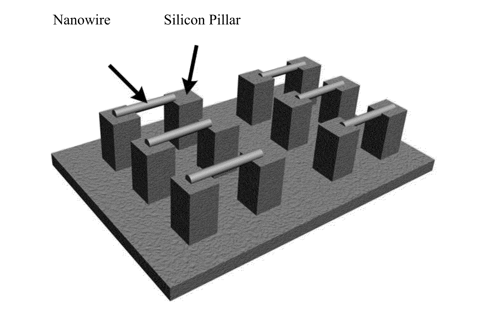
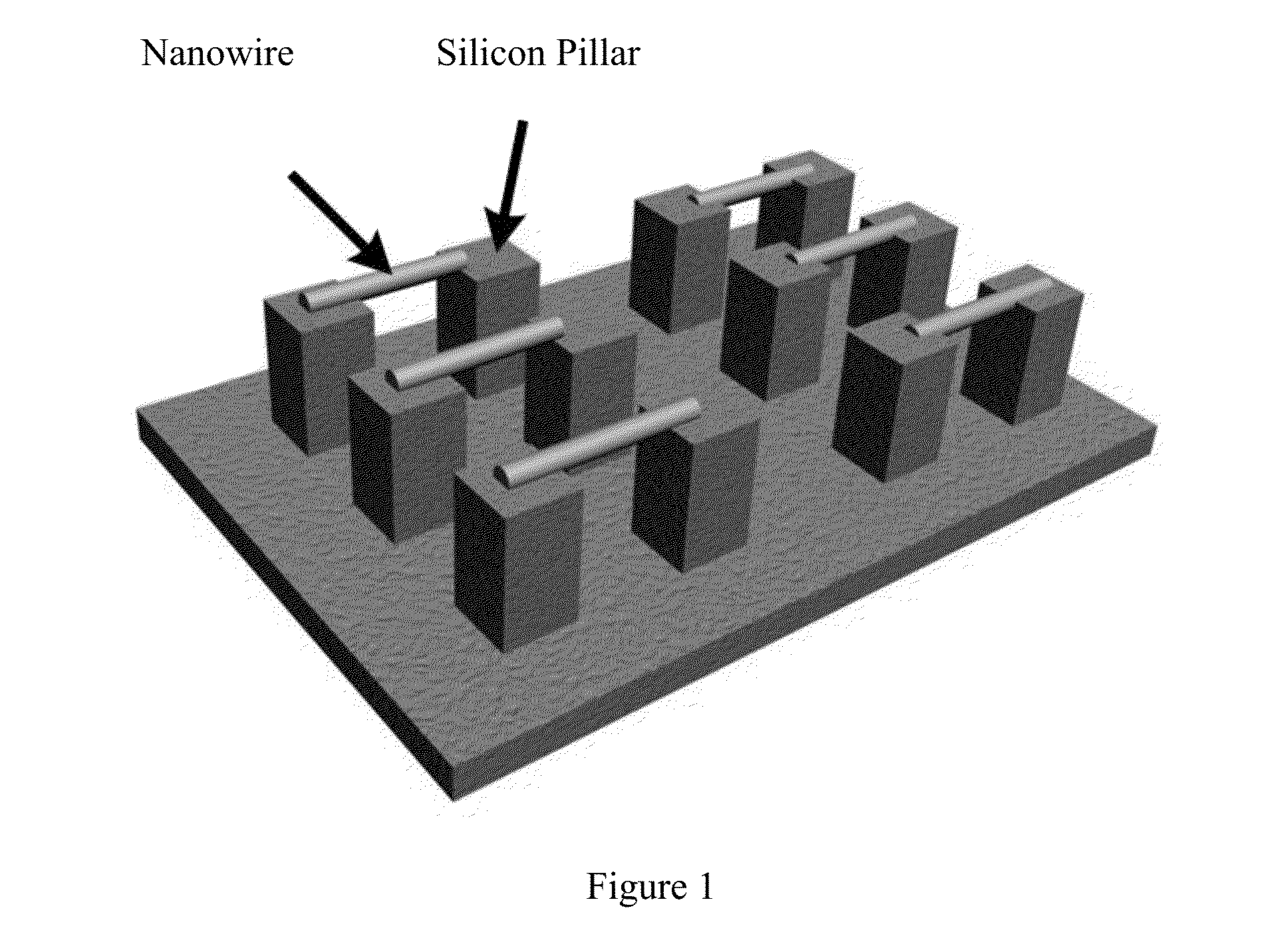
[0034](1) Immerse a silicon wafer with a hydrophilic silicon pillar array on the surface prepared through a laser etching process (the interval between adjacent silicon pillars in the array is 15 μm, the silicon pillars are in micrometer-level diameter) into 1 wt % ethanol solution of fluorooctylsilane, and control the silicon wafer and the molecules of fluorooctylsilane to have grafting reaction for 12 h so that the surface of the silicon wafer is modified by the molecules of fluorooctylsilane, to obtain a silicon wafer that contains a hydrophobic silicon pillar array (the silicon pillars in the array is in micrometer-level diameter);

[0035](2) Utilize gravity action to drive 1 wt % water solution of polyvinyl alcohol adulterated with nanometer copper particles in 10 nm particle size (the mass ratio of polyvinyl alcohol to nanometer copper particles is 1:5) to flow across the top surface of the hydrophobic silicon pillar array on the silicon wafer obtained in step (1) at 5 ...

Example

Example 2

[0038](1) Immerse a silicon wafer with a hydrophilic silicon pillar array on the surface prepared through a masking and exposure process (the interval between adjacent silicon pillars in the array is 1 μm, the silicon pillars are in micrometer-level diameter) into 13% (mass percent) acetone solution of fluorodecylsilane, and control the silicon wafer and the molecules of fluorodecylsilane to have grafting reaction for 1 h so that the surface of the silicon wafer is modified by the molecules of fluorodecylsilane, to obtain a silicon wafer that contains a hydrophobic silicon pillar array (the silicon pillars in the array is in micrometer-level diameter);

[0039](2) Utilize adhesion induction technique to induce 1×10⁻⁹% (mass percent) water solution of poly(3,4-ethylenedioxythiophene) adhered to ordinary cotton rodlets to flow across the top surface of the hydrophobic silicon pillar array on the silicon wafer obtained in step (1) at 0.1 cm / s constant flow rate in a specific dire...

Example

Example 3

[0040](1) Immerse a silicon wafer with a hydrophilic silicon pillar array on the surface prepared through a wet chemical erosion process (the interval between adjacent silicon pillars in the array is 30 μm, the silicon pillars are in micrometer-level diameter) into 25% (mass percent) dimethyl sulfoxide solution of fluorododecylsilane, and control the silicon wafer and the molecules of fluorododecylsilane to have grafting reaction for 24 h so that the surface of the silicon wafer is modified completely by the molecules of fluorododecylsilane, to obtain a silicon wafer that contains a hydrophobic silicon pillar array (the silicon pillars in the array is in micrometer-level diameter);

[0041](2) Utilize magnetic field effect to drive 20% (mass percent) water solution of polystyrene sulfonate-poly(3,4-ethylenedioxythiophene) (PSS-PEDOT) to flow across the top surface of the hydrophobic silicon pillar array on the silicon wafer obtained in step (1) at a constant flow rate in a spe...


PUM

PropertyMeasurementUnit
Fractionaaaaaaaaaa
Fractionaaaaaaaaaa
Timeaaaaaaaaaa

Abstract

Provided is a method of forming large-area directionally aligned nanowires on a silicon wafer surface with hydrophobic silicon pillars so as to form microelectrode-pair arrays, which belongs to the field of electronic circuit. The method includes grafting fluoroalkylsilane on the surface of a silicon wafer with hydrophilic silicon pillar arrays; increasing the contact angle between the surface of the hydrophilic silicon pillar arrays and water from 10° to 150° above and obtaining the silicon wafer with hydrophobic silicon pillar arrays; driving water solution containing materials used for forming nanowires to flow across the surface with the hydrophobic silicon pillar arrays uniformly, so that directionally aligned nanowires are formed on the tops of each two adjacent silicon pillars in the hydrophobic silicon pillar arrays; each of the nanowires connects the two adjacent silicon pillars together so as to form a microelectrode-pair, and a plurality of microelectrode-pairs constitute the microelectrode-pair arrays.

Description

CROSS REFERENCE TO RELATED APPLICATIONS[0001]This application claims the priority to PCT Application No. PCT / CN2011 / 072446, filed on Apr. 2, 2011, entitled “Method for Forming Microelectrode-Pair Arrays on Silicon Substrate Surface with Hydrophobic Silicon Pillars”, which is specifically and entirely incorporated by reference.FIELD OF THE INVENTION[0002]The present invention belongs to the field of electronic circuit, and particularly relates to a method for forming a large-area of nanowires in a directional arrangement on the surface of a silicon wafer with hydrophobic silicon pillars and thereby building up an array of microelectrode pairs.BACKGROUND OF THE INVENTION[0003]Microelectrodes are electrodes with micrometer-level (1×10⁻⁶ m) to nanometer-level (1×10⁻⁹ m) linear dimension. As the linear dimension of an electrode is reduced from millimeter level to micrometer level, the electrode will exhibit many outstanding electro-chemical properties. For example, thanks to the tiny ele...

Claims


Application Information

Patent Timeline
IPC IPC(8): B81C1/00
CPCB81C1/00341H01L29/125B82Y30/00B82Y10/00B81C1/00206B81B2203/0361B82Y40/00H01L29/41725H01L29/66439H01L29/0649H01L29/0673H01L29/16H01L29/413B05D1/18B05D5/12C23C18/04C23C18/18B05D1/02C23C18/31
Inventor JIANG, LEISU, BINWANG, SHUTAOMA, JIESONG, YANLIN
Owner INST OF CHEM CHINESE ACAD OF SCI
Why Eureka
Try Eureka