Optical navigation device

Active Publication Date: 2014-04-24
STMICROELECTRONICS RES & DEV
View PDF2 Cites 3 Cited by
  • Summary
  • Abstract
  • Description
  • Claims
  • Application Information

AI Technical Summary

Benefits of technology

The patent describes a method for improving the input of user input devices by illuminating a surface to a sufficient degree using a laser. The angle between the laser and the surface should be between 30 degrees and 40 degrees for optimal performance. The use of a relatively cheap and widely available laser diode and optical element can make the device more compact and cost-effective. Additionally, reflective coatings are not necessary because the laser light is internally reflected by the surface. This method simplifies the manufacturing process and reduces the likelihood of mistakes.

Problems solved by technology

It will be understood that, when a user touches the exposed user surface with an object (e.g., a human digit or a stylus), total internal reflection at the second TIR surface may be frustrated, leading to a pattern being formed on the imaging surface.

Method used


Image

  • Optical navigation device
  • Optical navigation device
  • Optical navigation device

Examples


Embodiment Construction

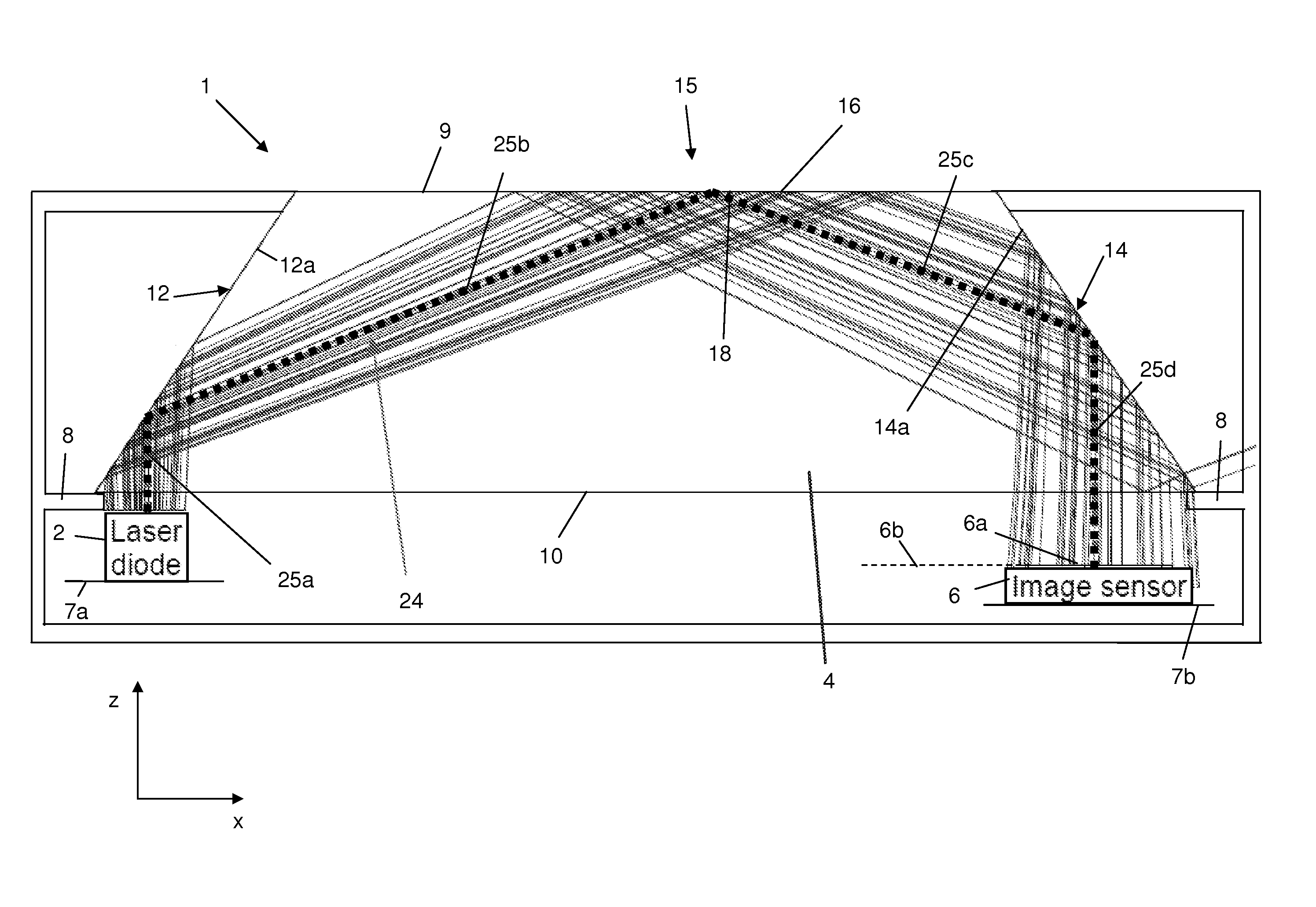
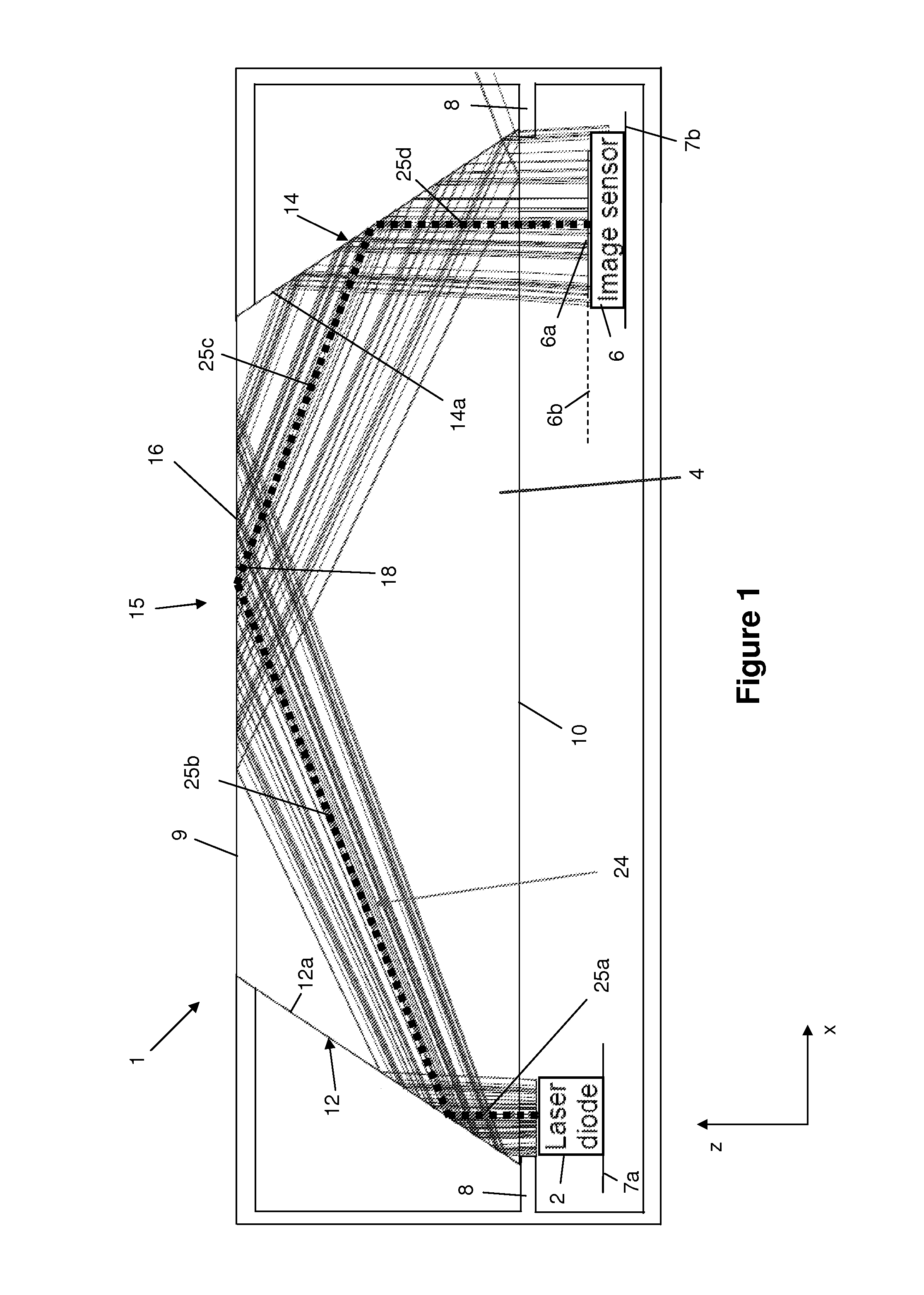
[0049]FIG. 1 is a schematic cross sectional view of an optical navigation device 1 comprising a laser diode 2 (typically a VCSEL but may be any other suitable type of laser diode), an optical element 4 and an image sensor 6 having a substantially planar imaging surface 6a lying on an imaging plane 6b. The laser diode 2 and image sensor 6 are mounted on separate circuit boards 7a, 7b, while the optical element 4 is suspended above the circuit boards 7a, 7b by a supportive housing 8. It will be understood that the laser 2 and image sensor 6 may alternatively be mounted on the same circuit board.

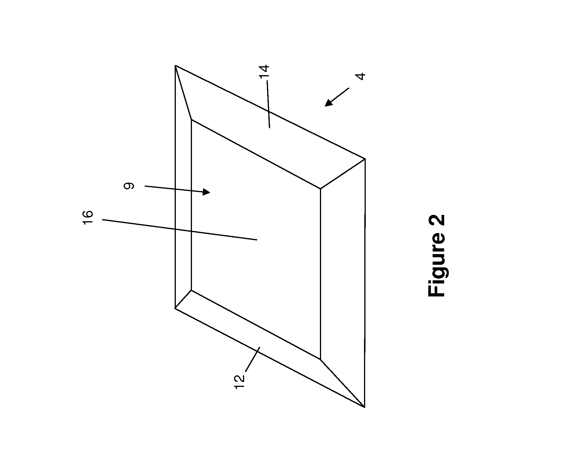
[0050]As shown in FIGS. 1 and 2, the optical element 4 comprises an upper, user input face 9 and a lower face 10 with a pair of angled side faces 12, 14 extending between them, the side faces 12, 14 converging towards each other as they extend from the lower face 10 to the upper face 9. A touch sensitive input area 15 is formed at an intermediate region of the user input face 9 between the angl...


PUM


Abstract

An optical navigation device for use with mobile telephones and the like is disclosed, which has a reduced height as compared with current designs. The navigation device comprises a laser such as a VCSEL laser, an exposed user surface and two other surfaces that provide for total internal reflection of the incident laser beam. The surfaces are constructed with shallower than normal angles, preserving the basic functionality of the device while reducing the height.

Description

BACKGROUND[0001]1. Technical Field[0002]The disclosure relates to an optical navigation device, a method of manufacturing an optical navigation device, a mobile communications device comprising an optical navigation device and a method of operating an optical navigation device.[0003]2. Description of the Related Art[0004]Current mobile or computer devices use a variety of different navigation mechanisms including trackball devices, multi-click joysticks and capacitance based touch areas. However, there are problems associated with each of these. Trackballs and joysticks can be unreliable and relatively expensive to implement. In addition, capacitance based touch areas do not operate satisfactorily if the finger is covered, for example by a glove, and their size can be large in relation to devices such as mobile phones and PDAs.[0005]Optical navigation devices are also known which operate on the same principals as optical mice by comparing successive frames of an area image. However,...

Claims


Application Information

Patent Timeline
IPC IPC(8): G06F3/0354H01L25/16
CPCH01L25/167G06F3/03547G06F3/0421H01L2924/0002H01L2924/00
Inventor CAMPBELL, COLINMCINNES, HAZELFINDLAY, EWAN
Owner STMICROELECTRONICS RES & DEV
Why Eureka
Try Eureka