

Cascode amplifier
a technology of cascode amplifier and cascode, which is applied in the direction of amplifiers, amplifiers with semiconductor devices only, amplifiers with semiconductor devices, etc., can solve the problems that the total gate width may not result in an increase in the output power of power amplifiers or cascode amplifiers, and achieve the effect of minimizing the reduction of their output power
- Summary
- Abstract
- Description
- Claims
- Application Information
AI Technical Summary
Benefits of technology
Problems solved by technology
Method used
Image

Examples
first embodiment
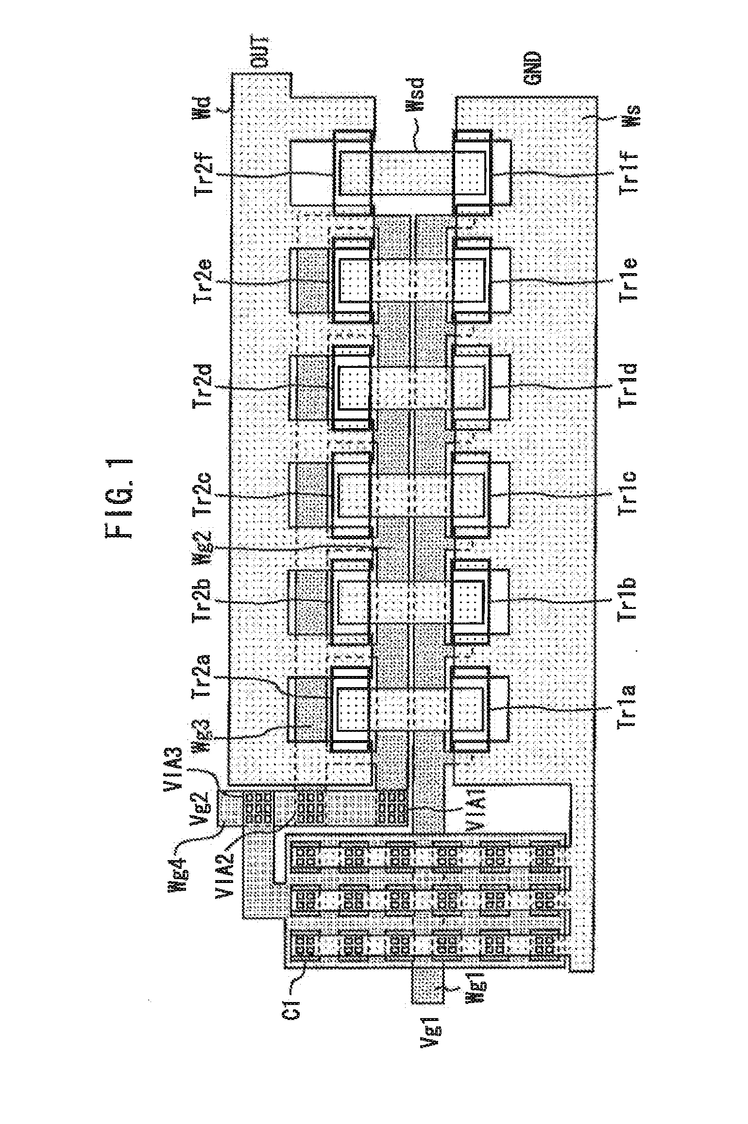
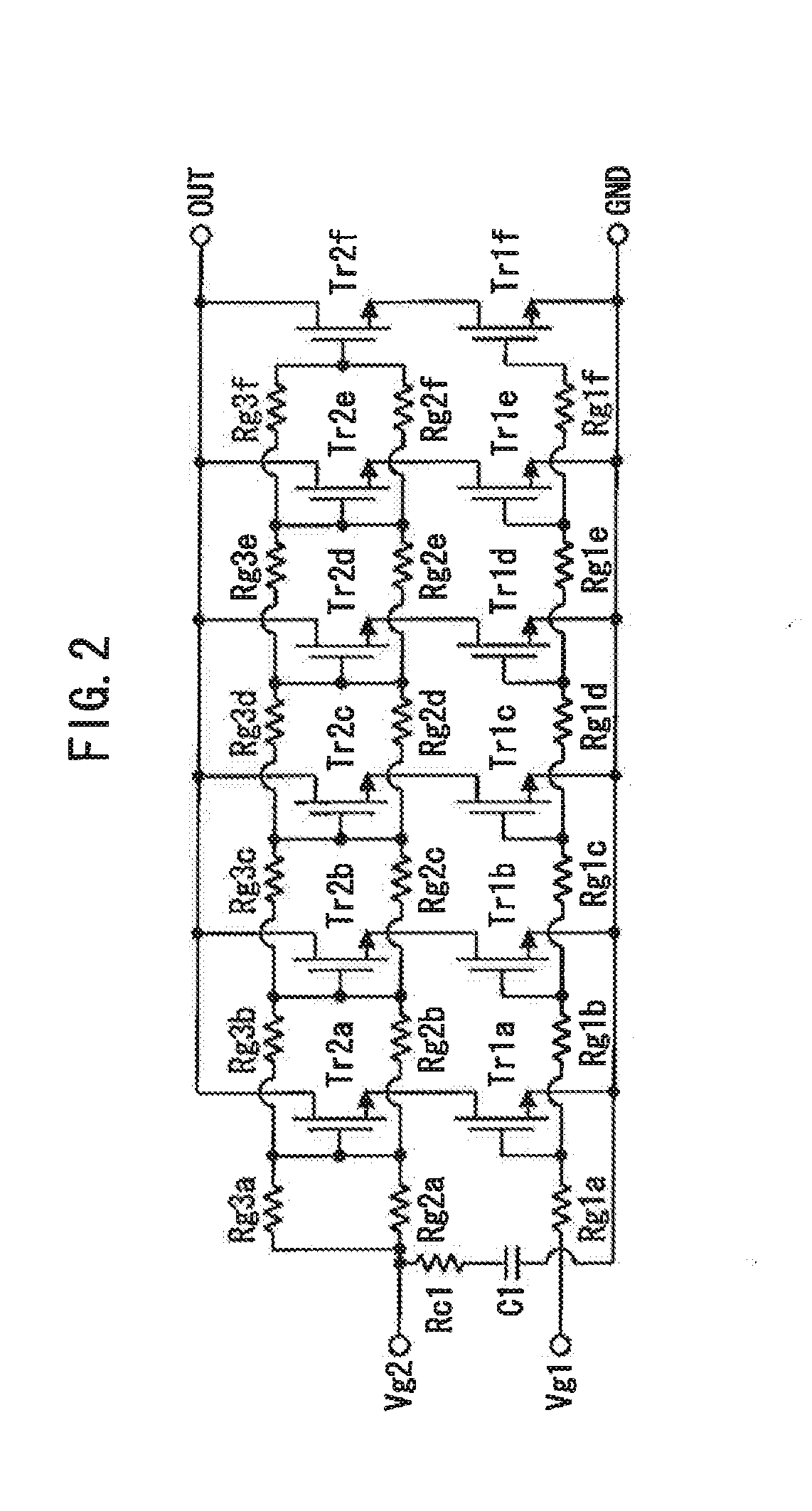
[0030]FIG. 1 is a top view of a cascode amplifier in accordance with a first embodiment of the present invention. FIG. 2 is a circuit diagram of the cascode amplifier of the first embodiment. Transistors Tr1a to Tr1f are cascode-connected with transistors Tr2a to Tr2f, respectively. These transistors are n-channel MOS transistors.
[0031]A line Wg1 is connected at spaced points along its length to the gates of the transistors Tr1a to Tr1f. A line Wg2 and a line Wg3 are connected at spaced points along their length to the gates of the transistors Tr2a to Tr2f. The lines Wg2 and Wg3 are connected in parallel with each other. One end of a capacitance C1 is connected to one end of the line Wg2 and one end of the line Wg3, and the other end of the capacitance C1 is connected to GND.
[0032]The sources of Tr1a to Tr1f are connected through a line Ws to GND. The drains of Tr1a to Tr1f are connected through lines Wsd to the sources of Tr2ato Tr2f, respectively. The drains of Tr2a to Tr2f are co...
second embodiment
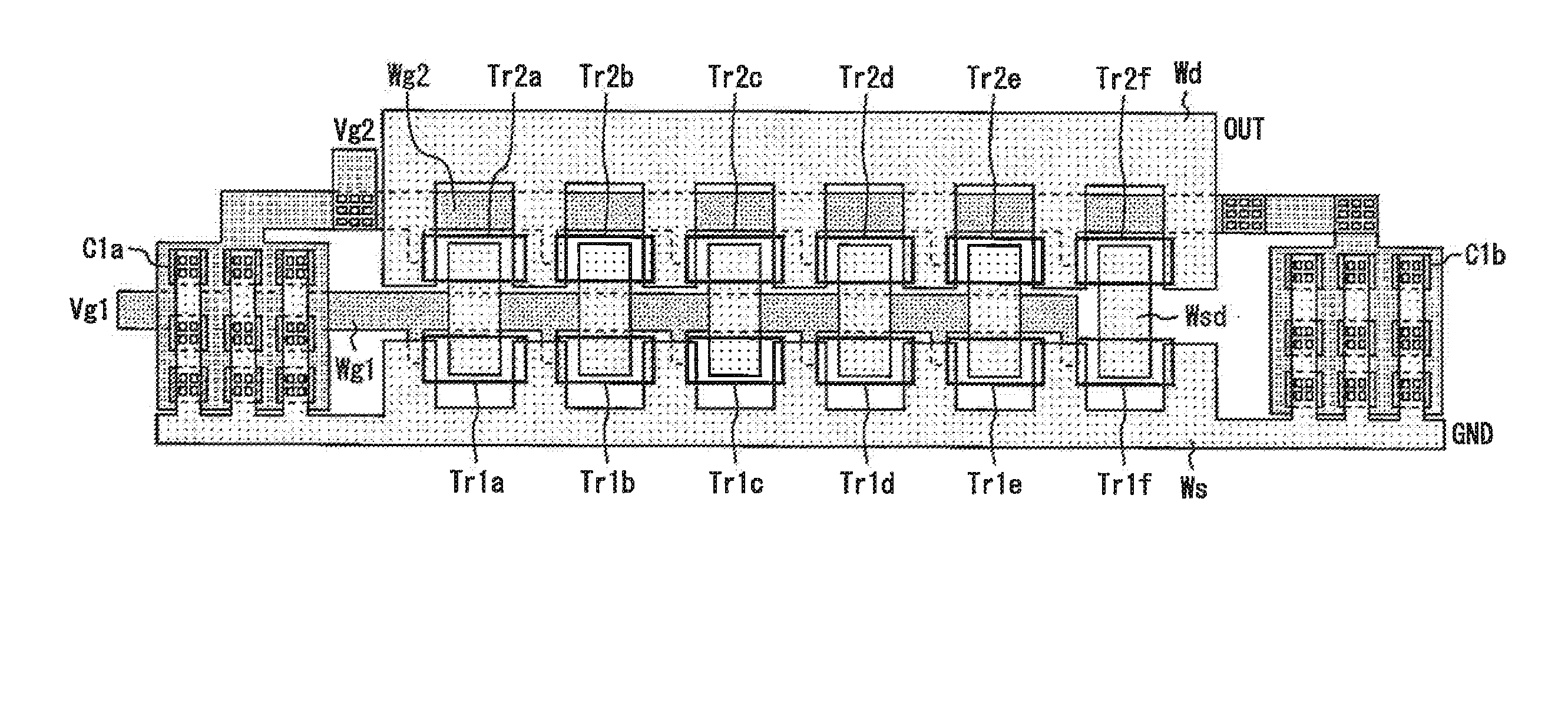
[0045]FIG. 10 is a top view of a cascode amplifier in accordance with a second embodiment of the present invention. FIG. 11 is a circuit diagram of the cascode amplifier of the second embodiment. In the cascode amplifier of the second embodiment, unlike that of the first embodiment, a first capacitance C1a is connected between one end of the line Wg2 and ground and a second capacitance C1b is connected between the other end of the line Wg2 and ground. A resistance Rc1a represents the sum of the parasitic resistances of the line and vias connected in series between the Vg2 terminal and the first capacitance C1a. A resistance Rc1b represents the sum of the parasitic resistances of the line and vias connected in series between the gate of Tr2f and the second capacitance C1b.
[0046]The cascode amplifier of the present embodiment is provided with two RF grounding capacitances, namely the first capacitance C1a and the second capacitance C1b, instead of only one RF grounding capacitance (a...
third embodiment
[0047]FIG. 12 is a top view of a cascode amplifier in accordance with a third embodiment of the present invention. FIG. 13 is a circuit diagram of the cascode amplifier of the third embodiment. In the cascode amplifier of the third embodiment, unlike that of the first embodiment, capacitances C1a to C1f are connected at one end to the gates of the transistors Tr2a to Tr2f by lines Wg5a to Wg5f, respectively, and connected at the other end to GND. Resistances Rc1a to Rc1f (see FIG. 13) represent the sum of the parasitic resistances of the line and vias connected in series between the capacitances C1a to C1f and the gates of the transistors Tr2a to Tr2f, respectively; specifically, the resistance Rc1a represents the sum of the parasitic resistances of the line Wg5a and vias by which the capacitance C1a is connected to the gate of the transistor Tr2a, the resistance Rc1b represents the parasitic resistances of the line Wg5b and vias by which the capacitance C1b is connected to the gate...
PUM
 Abstract
Description
Claims
Application Information