High-Resolution Molecular Sensor

a molecular sensor, high-resolution technology, applied in the field of nanoscale devices, can solve the problems of inability to achieve single nucleotide sensitivity, inability to discriminate, and small ionic current differences resulting from the translocation of different dna bases

Active Publication Date: 2014-06-19
PRESIDENT & FELLOWS OF HARVARD COLLEGE
View PDF1 Cites 14 Cited by
  • Summary
  • Abstract
  • Description
  • Claims
  • Application Information

AI Technical Summary

Benefits of technology

This patent describes a molecular sensing device that can detect individual molecules, such as DNA and RNA, with high accuracy. The device has a special structure that allows for the molecule to pass through a small aperture in the device and an electrical current to be measured as it passes. This makes it easy to measure the changes in the molecule's electrical properties as it moves through the device. Overall, this device is much better than previous molecular sensors and can detect even small amounts of molecules. This technology is useful for studying biomolecules and their interactions.

Problems solved by technology

But the small ionic current differences resulting from the translocation of different DNA bases are generally beyond the resolution limit of conventional current amplifiers because the intrinsic noise due to the charged DNA bases is so large, and it is therefore not possible to discriminate between specific bases.
While such configurations are expected to provide an improved signal-to-noise ratio, they cannot, in general, achieve single nucleotide sensitivity.

Method used


Image

  • High-Resolution Molecular Sensor
  • High-Resolution Molecular Sensor
  • High-Resolution Molecular Sensor

Examples


Embodiment Construction

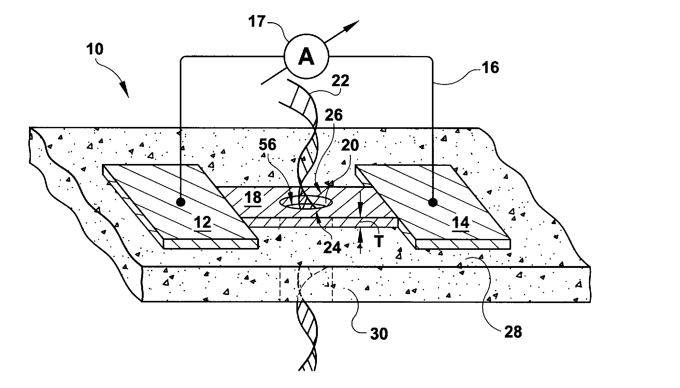
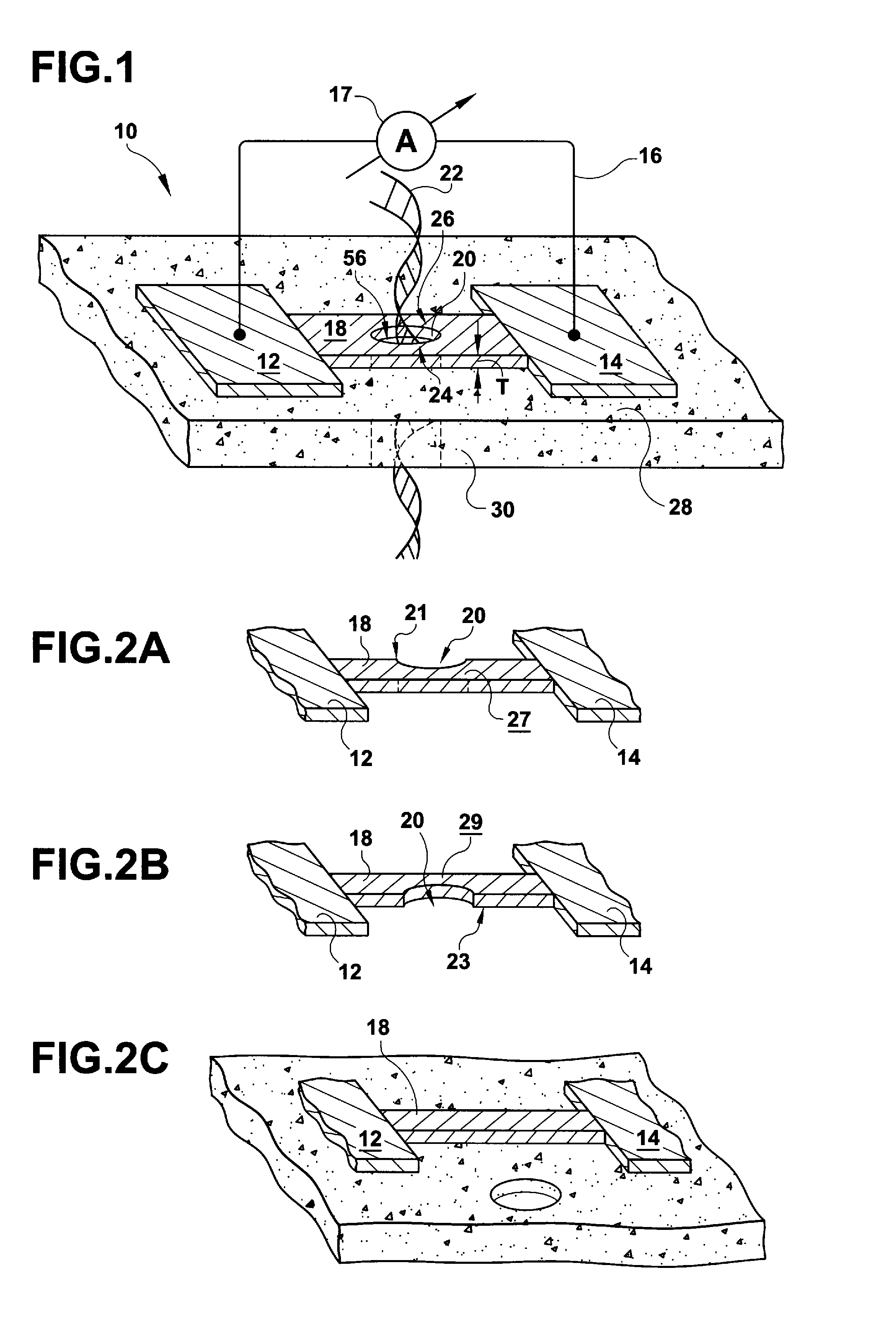
[0013]Referring to FIG. 1, there is schematically represented an example implementation of the nanoscale sensor 10 of the invention. In this example, there is provided a field-effect transistor (FET) configuration in which an electrically conducting source region 12 and an electrically conducting drain region 14 are connected in a sensing circuit 16. Electrical current is injected and collected between the source and drain through a molecular sensing channel region 18. The molecular sensing channel region includes an aperture 20, preferably a nanopore, that is disposed centrally, at an edge of, or just adjacent to, the channel region. In the example of FIG. 1, the nanopore aperture is provided generally centrally to the channel region 18. Other aperture arrangements are described below. The channel region and source and drain regions are provided on a support structure 28 having an aperture 30 through the thickness thereof that is in communication with the nanopore 20 of the channel...


PUM


Abstract

A solid state molecular sensor having an aperture extending through a thickness of a sensing material is configured with a continuous electrically-conducting path extending in the sensing material around the aperture. A supply reservoir is connected to provide a molecular species, having a molecular length, from the supply reservoir to an input port of the aperture. A collection reservoir is connected to collect the molecular species from an output port of the aperture after translocation of the molecular species from the supply reservoir through the sensing aperture. The sensing aperture has a length between the input and output ports, in the sensing material, that is substantially no greater than the molecular length of the molecular species from the supply reservoir. An electrical connection to the sensing material measures a change in an electrical characteristic of the sensing material during the molecular species translocation through the aperture.

Description

CROSS-REFERENCE TO RELATED APPLICATIONS[0001]This application is a divisional of copending U.S. application Ser. No. 12 / 667,573, filed Jun. 28, 2010, the entirety of which is hereby incorporated by reference. U.S. application Ser. No. 12 / 667,573, in turn is a national stage application under 35 U.S.C. §371 of International Application No. PCT / US08 / 10637, filed Sep. 12, 2008, which claims the benefit of U.S. Provisional Application No. 60 / 993,388, filed Sep. 12, 2007, the entirety of all of which are hereby incorporated by reference.STATEMENT REGARDING FEDERALLY SPONSORED RESEARCH[0002]This invention was made with Government support under Contract No. FA8650-06-C-7622, and No. FA8560-06-C-7618, awarded by DARPA. The Government has certain rights in the invention.BACKGROUND OF INVENTION[0003]This invention relates generally to nanoscale devices, and more particularly relates to nanoscale devices for detecting and analyzing species such as molecules components of molecules.[0004]The de...

Claims


Application Information

Patent Timeline
Patent Type & Authority Applications(United States)
IPC IPC(8): G01N27/447
CPCB82Y15/00H01L29/1606G01N27/4145G01N33/48721
Inventor LIEBER, CHARLES M.XIONG, QIHUAXIE, PINGFANG, YING
Owner PRESIDENT & FELLOWS OF HARVARD COLLEGE
Why Eureka
Try Eureka