Anti-aliasing sampling circuits and analog-to-digital converter

a sampling circuit and anti-aliasing technology, applied in analogue/digital conversion, transmission systems, instruments, etc., can solve the problems of reducing the adc output full scale, wasting substantial power, and difficulty in providing a filter with a sharp cuto

Active Publication Date: 2014-06-19
ANALOG DEVICES INT UNLTD
View PDF2 Cites 15 Cited by
  • Summary
  • Abstract
  • Description
  • Claims
  • Application Information

AI Technical Summary

Problems solved by technology

However, it is difficult to provide a filter with a sharp cutoff before the ADC 203.
However, in conjunction with increased computational power, the need for a faster ADC to oversample the input signal wastes substantial power.
Configuration in this manner may result in a reduced ADC output full scale.
For example, if a gain of 8× is desired, one could use a 35 p sampling capacitor in conjunction with the SA Cap array; however, such a large capacitance may be impractical or undesired.

Method used


Image

  • Anti-aliasing sampling circuits and analog-to-digital converter
  • Anti-aliasing sampling circuits and analog-to-digital converter
  • Anti-aliasing sampling circuits and analog-to-digital converter

Examples


Embodiment Construction

[0034]In the following detailed description, numerous specific details are set forth by way of examples in order to provide a thorough understanding of the relevant teachings. However, it should be apparent to those skilled in the art that the present teachings may be practiced without such details. In other instances, well known methods, procedures, components, and / or circuitry have been described at a relatively high-level, without detail, in order to avoid unnecessarily obscuring aspects of the present teachings.

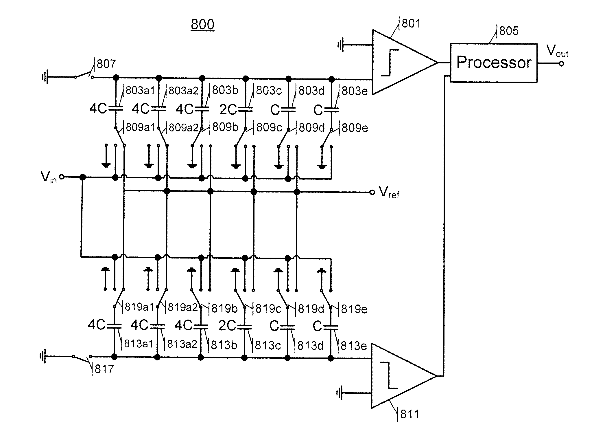
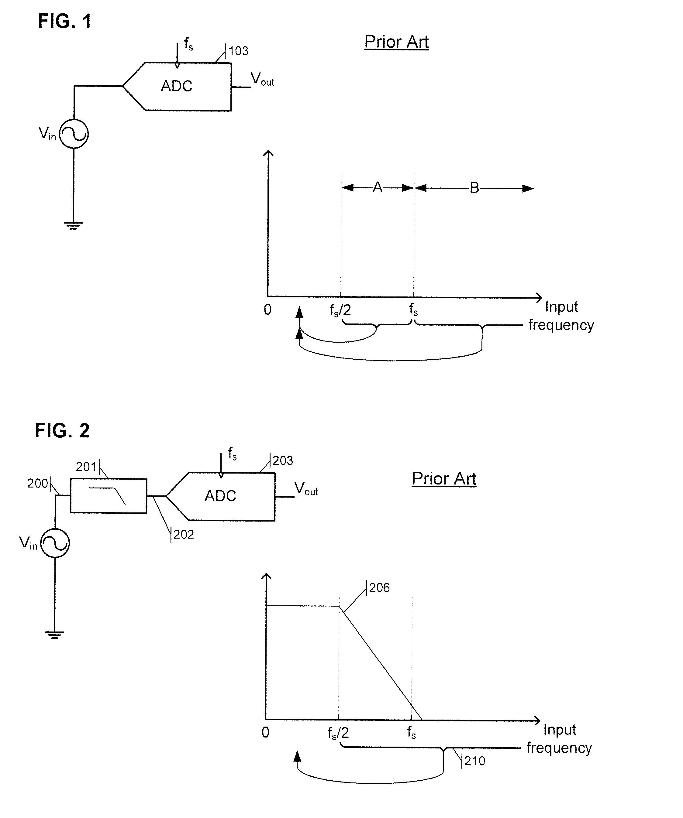
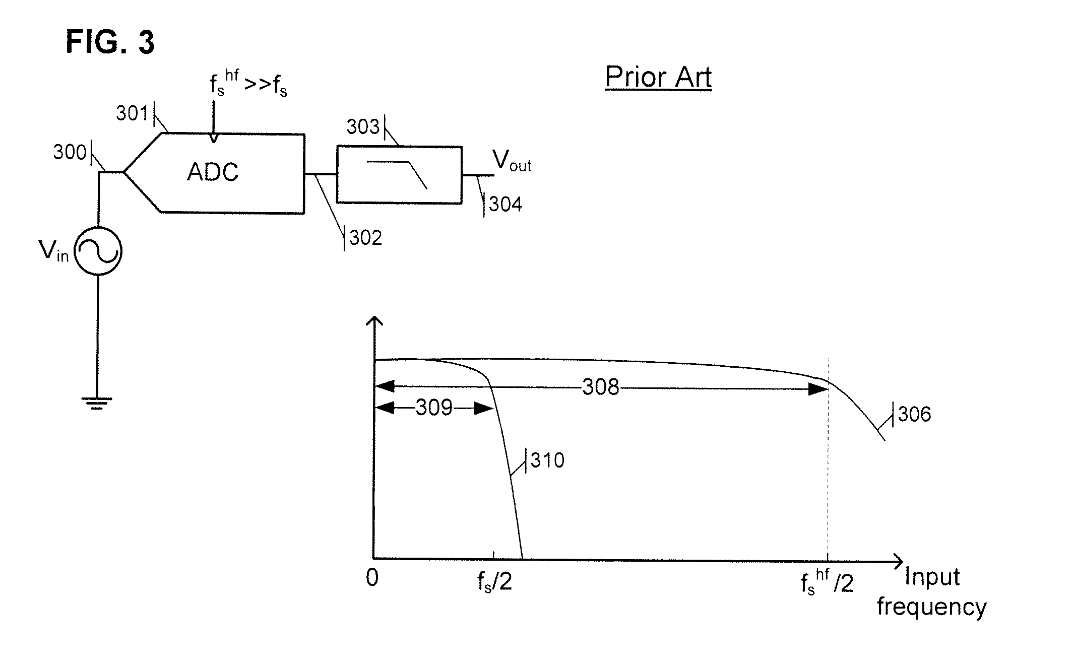
[0035]The various methods and circuits disclosed herein relate to improving the accuracy and reducing the noise sensitivity of sampling circuits, such as sampling circuits forming part of analog-to-digital converters. The methods and circuits increase the effective rate at which an input signal is sampled and, by recombining charge across capacitors or other storage devices used for sampling, provide anti-aliasing filtering of the input signal. In the case of analog-to-di...


PUM


Abstract

A sampling circuit, such as the sampling circuit of a successive approximation analog-to-digital converter (ADC), provides anti-aliasing filtering of a sampled input signal. The circuit samples the input signal using multiple capacitors, wherein each capacitor samples the input signal at a distinct time during a sampling time interval. The circuit combines the samples stored on different capacitors during a conversion time interval, and generates a digital output signal using the combined samples. In one example, a first bit of the output signal is generated using a sample stored on a first capacitor, and second bit of the output signal is generated using a sample stored on a second capacitor. In another example, the circuitry performs finite or infinite impulse response (FIR or IIR) filtering of the input signal, where a filter characteristic is determined by the relative sizes of the capacitors used for sampling.

Description

TECHNICAL FIELD[0001]The present subject matter relates to techniques and equipment for improving the accuracy and reducing the noise sensitivity of sampling circuits, such as sampling circuits forming part of analog-to-digital converters.BACKGROUND[0002]A sampling circuit, such as an analog to digital converter (ADC), converts a continuous time signal into a discrete time signal formed of a sequence of discrete signal samples. In the case of an ADC, each discrete signal sample is further digitized into a binary string representative of the discrete signal sample value to form a digital output signal. The sampling circuit commonly uses a capacitor (or other charge storage device) to sample the continuous time input signal value at a given instant in time. The sampling circuit passes the sampled signal value to a conversion circuit, or otherwise makes use of the sampled signal value stored on the capacitor.[0003]The sampling circuit operates at a determined sampling rate fs to take o...

Claims


Application Information

Patent Timeline
Patent Type & Authority Applications(United States)
IPC IPC(8): H03M1/12
CPCH03M1/124H03M1/1245H03M1/468
Inventor LEMKIN, MARK ALAN
Owner ANALOG DEVICES INT UNLTD
Why Eureka
Try Eureka