Pixel circuit, electro-optic device, and electronic apparatus

a technology of electrooptic devices and pixel circuits, applied in the direction of instruments, static indicating devices, etc., can solve the problems of increasing production costs or decreasing yields, and achieve the effect of reducing the size and weight of the devi

Inactive Publication Date: 2014-06-19
SEIKO EPSON CORP
View PDF4 Cites 4 Cited by
  • Summary
  • Abstract
  • Description
  • Claims
  • Application Information

AI Technical Summary

Benefits of technology

[0011]An advantage of some aspects of the invention is to provide a high-precision 2-screen display device with a simple and easy configuration.

Problems solved by technology

To realize the 2-screen displaying without decreasing the definition display as compared with a general 1-screen display device, it is necessary to arrange the pixels with double density, and a problem of increasing production cost or decreasing yields occurs due to complication of the production process.

Method used


Image

  • Pixel circuit, electro-optic device, and electronic apparatus
  • Pixel circuit, electro-optic device, and electronic apparatus
  • Pixel circuit, electro-optic device, and electronic apparatus

Examples


first embodiment

A: First Embodiment

[0059]Hereinafter, various embodiments according to the invention will be described with reference to the accompanying drawings. In the drawings, the dimensions and ratios of sections are appropriately different from those of the real things.

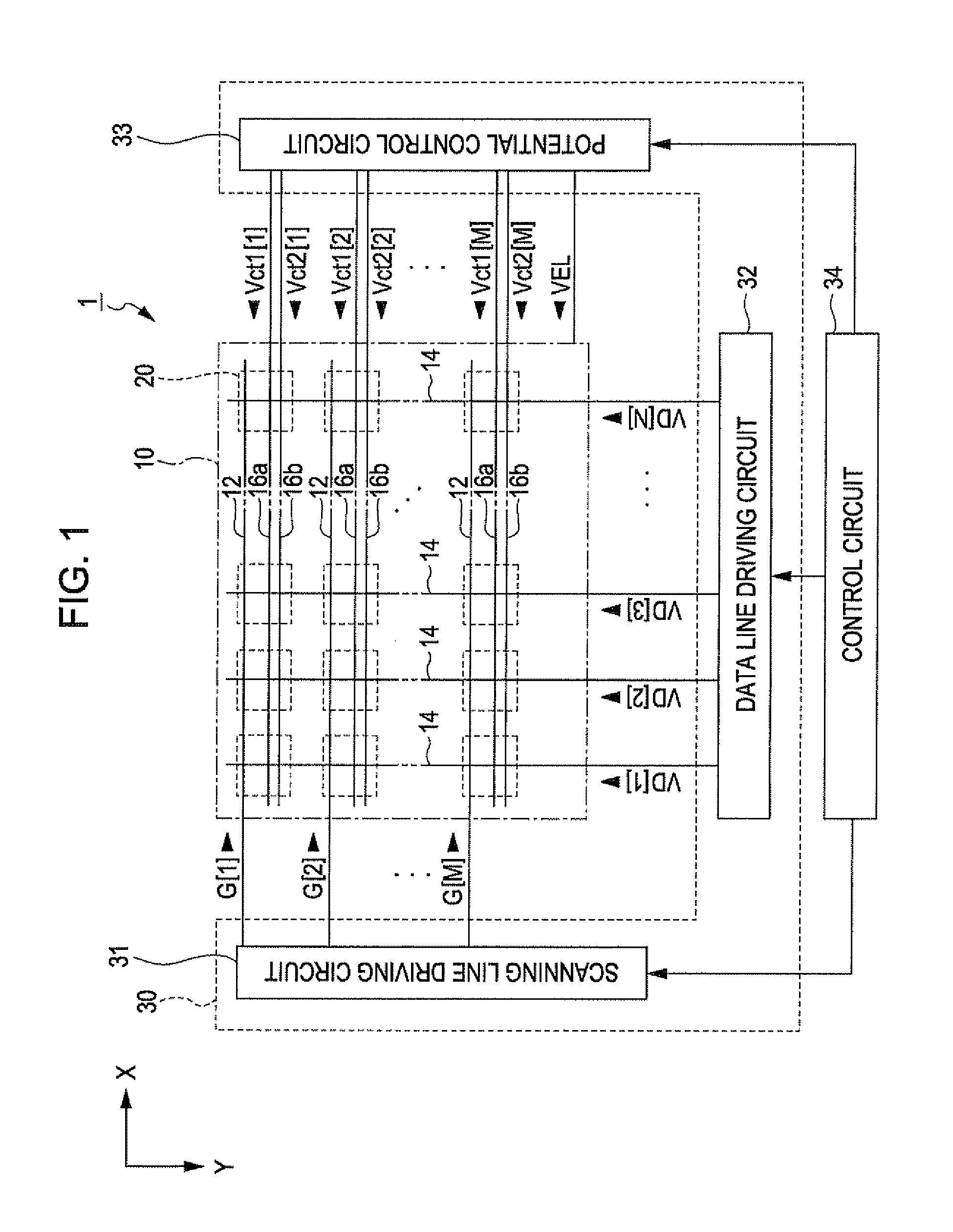
[0060]FIG. 1 is a block diagram illustrating a display device 1 according to a first embodiment of the invention.

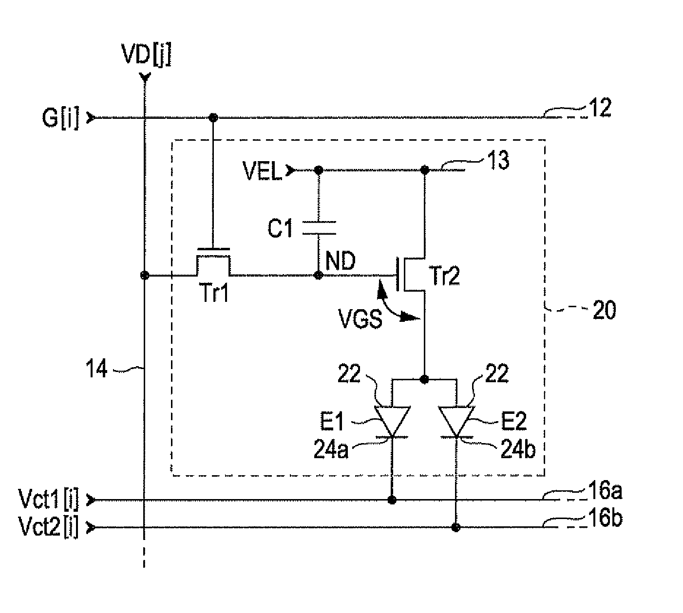
[0061]The display device 1 includes a display area 10 in which a plurality of pixel circuits 20 are arranged, and a driving circuit 30 driving the pixel circuits 20. For example, the driving circuit 30 is dispersedly mounted on a plurality of integrated circuits. However, at least a part of the driving circuit 30 may be formed of a thin-film transistor formed on a substrate with the pixel circuits 20.

[0062]In the display area 10, M scanning lines 12 extending in the X direction, M first power supply lines 16a and M second power supply lines 16b extending in the X direction, and N data lines 14 extending in the Y dir...

second embodiment

B: Second Embodiment

[0128]FIG. 10 is a block diagram illustrating disposition of pixel circuits 20 and opposed electrodes 24 according to a second embodiment. A display device 1A of the second embodiment has the same configuration as that of the display device 1 of the first embodiment, except that an opposed electrode 24 is provided instead of the first opposed electrode 24a and the second opposed electrode 24b, and a power supply line 16 is provided instead of the first power supply line 16a and the second power supply line 16b.

[0129]As shown in FIG. 10, each pixel circuit 20 of the display device 1A is provided with a light emission layer 23 having a rectangular shape formed of long sides parallel to the Y axis and short sides parallel to the X axis.

[0130]The opposed electrodes 24 have a rectangular shape formed of long sides parallel to the X axis and short sides parallel to the Y axis, and are provided to be common for N first light emitting devices E1 provided in N pixel circ...

modified example 1

1. Modified Example 1

[0153]In the first embodiment and the second embodiment described above, each pixel circuit 20 is provided with the capacitor C1, one electrode of which is electrically connected to the first node ND, and the other electrode of which is electrically connected to the third power supply line 13. However, the invention is not limited to such a configuration, and a pixel circuit 20A shown in FIG. 14 may be used instead of the pixel circuit 20.

[0154]The pixel circuit 20A is provided with a capacitor C2, one electrode of which is electrically connected to the first node ND, and the other electrode of which is electrically connected to the second node ND2 positioned between the source of the driving transistor Tr2 and the common electrode 22. The pixel circuit 20A keeps the image signal VD [i, j] supplied from the data line 14, by the capacitor C2. Even after the selection signal G [i] becomes the low level, the first light emitting device E1 and the second light emitt...


PUM


Abstract

A pixel circuit includes a first light emitting device including a common electrode and a first opposed electrode connected to a first power supply line, and a second light emitting device including the common electrode and a second opposed electrode connected to the second power supply line. A first potential and a second potential are alternately supplied to a first power supply potential supplied to the first power supply line and a second power supply potential supplied to the second power supply line, and thus the first light emitting device and the second light emitting device alternately emit light.

Description

[0001]The present application claims is a divisional application of U.S. patent application Ser. No. 13 / 267,452, filed Oct. 6, 2011, which claims priority from Japanese Patent Application No. 2010-236194, filed in the Japanese Patent Office on Oct. 21, 2010, the disclosure of each of which is hereby incorporated by reference in its entirety.BACKGROUND[0002]1. Technical Field[0003]The present invention relates to a pixel circuit provided with a light emitting device such as an organic EL (Electroluminescence) device, an electro-optic device including a display device or a lighting device having the pixel circuit, and an electronic apparatus provided with the electro-optic device.[0004]2. Related Art[0005]Recently, demand for 2-screen display devices displaying two different images on the left and right, or 3D displays performing 3D display by simultaneously outputting a left eye image and a right eye image, has increased along with the spread of car navigation systems having a 2-scre...

Claims


Application Information

Patent Timeline
Patent Type & Authority Applications(United States)
IPC IPC(8): G09G3/32
CPCG09G3/003G09G3/3225G09G2300/0866G09G3/3258H10K50/19
Inventor KUBOTA, TAKEHIKOFUJITA, SHIN
Owner SEIKO EPSON CORP
Why Eureka
Try Eureka