
Detecting apparatus, wafer and electronic device

a detection apparatus and electronic device technology, applied in the direction of resistance/reactance/impedence, semiconductor/solid-state device testing/measurement, instruments, etc., can solve the problems of low measurement speed and difficulty in improving measurement accuracy

Active Publication Date: 2014-07-17
THE UNIV OF TOKYO +1
View PDF4 Cites 4 Cited by
  • Summary
  • Abstract
  • Description
  • Claims
  • Application Information

AI Technical Summary

Benefits of technology

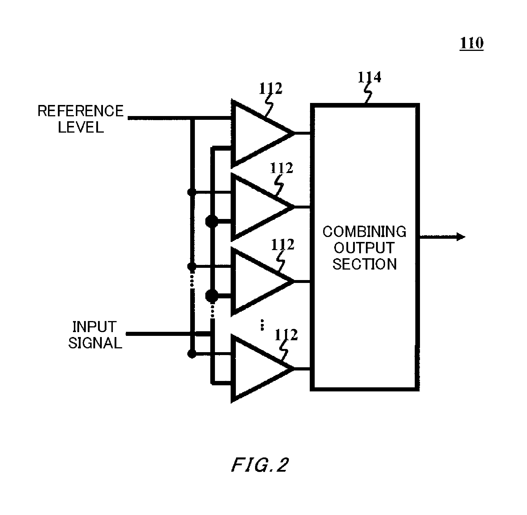
The present invention provides a detection apparatus, a wafer, and an electronic device that can overcome the process variation-related problems in the related art. The detection apparatus includes a signal input section and a detecting section that sequentially changes the signal level of an input signal and detects the process variation based on the distribution of the number of comparison results that indicate a predetermined result. The wafer includes a plurality of comparators that output a comparison result and a combining output section that combines the comparison results. The electronic device includes a plurality of comparators and a combining output section that combines the comparison results. This invention allows for more accurate and reliable detection and control of process variations in semiconductor devices.

Problems solved by technology

However, since an AC signal is being measured, the measurement is easily affected by jitter and there is a non-linear relationship between the threshold voltage and the oscillation frequency, and therefore it is difficult to improve the measurement accuracy.
Furthermore, in the method of Document 2, information is exchanged through the scan chain, and therefore the measurement speed is low.

Method used


Image

  • Detecting apparatus, wafer and electronic device
  • Detecting apparatus, wafer and electronic device
  • Detecting apparatus, wafer and electronic device

Examples


Embodiment Construction

[0020]Hereinafter, some embodiments of the present invention will be described. The embodiments do not limit the invention according to the claims, and all the combinations of the features described in the embodiments are not necessarily essential to means provided by aspects of the invention.

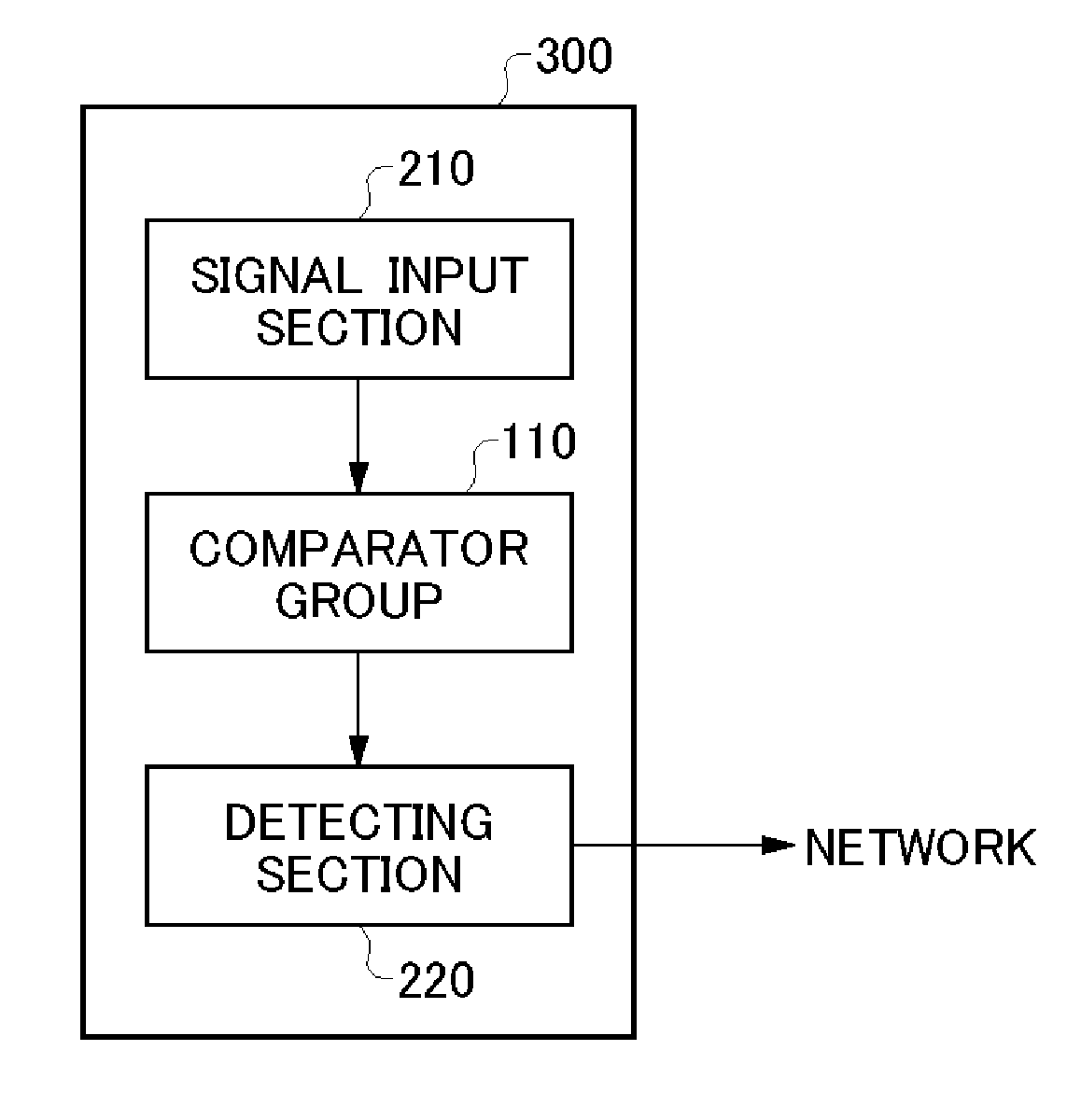
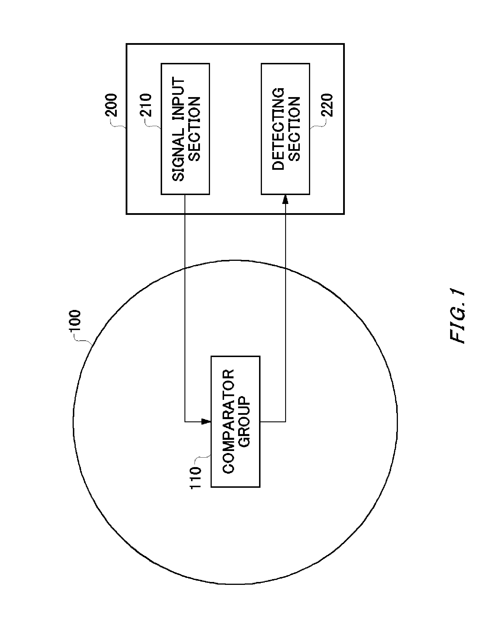
[0021]FIG. 1 shows an exemplary configuration of a detection apparatus 200 that detects process variation in a plurality of comparators. The detection apparatus 200 of the present embodiment detects process variation of the comparators included in a comparator group 110 formed on a semiconductor wafer 100. The detection apparatus 200 includes a signal input section 210 and a detecting section 220. The target of the process variation detection performed by the detection apparatus 200 is not limited to the semiconductor wafer 100. For example, the process variation can be detected in the same manner for a electronic device or the like including a comparator group 110.

[0022]The signal input sectio...


PUM


Abstract

Provided is a detection apparatus that detects process variation in a plurality of comparators that each output a comparison result obtained by comparing a signal level of an input signal to a reference level, the detection apparatus comprising a signal input section that inputs the input signal and the reference level in common to the comparators, and sequentially changes the signal level of the input signal; and a detecting section that detects, for each signal level, a number of comparison results that indicate a predetermined result, from among the comparison results of the comparators, and detects the process variation based on a distribution of the number of comparison results that indicate the predetermined result.

Description

BACKGROUND[0001]1. Technical Field[0002]The present invention relates to a detection apparatus, a wafer, and an electronic device.[0003]2. Related Art[0004]As a conventional method of detecting process variation in MOSFETs, a method using a rign oscillator (see Non-Patent Document 1) and a method using a sense amplifier (see Non-Patent Document 2) are known.[0005]Non-Patent Document 1: I. A. K. M. Mahfuzil, H. Onodera, “On-chip detection of process shift & process spread for silicon debugging and model-hardware correlation,” ATS2012.[0006]Non-Patent Document 2: S. Mukhopadhyay, K. Kim, K. A. Jenkins, C-T. Chuand, K. Roy, “Statistical Characterization and On-Chip Measurement Methods for Local Random Variability of a Process Using Sense-Amplifier-Based Test Structure,” ISSCC 2007, February 2007.[0007]The method of Document 1 includes measuring threshold voltages of an nMOSFET and a pMOSFET forming a ring oscillator, based on variation in the oscillation frequency of the ring oscillato...

Claims


Application Information

Patent Timeline
Patent Type & Authority Applications(United States)
IPC IPC(8): G01R31/28
CPCG01R31/2832H01L22/34G01R31/2894H01L2924/0002
Inventor YAMAGUCHI, TAKAHIROKOMATSU, SATOSHIASADA, KUNIHIROTANDON, JAMES SUMIT
Owner THE UNIV OF TOKYO
Learn More