Integrated circuit 3D phase change memory array and manufacturing method

a phase change memory and integrated circuit technology, applied in the direction of digital storage, instruments, electrical equipment, etc., can solve the problems of increasing costs and complicating manufacturing processes

Active Publication Date: 2014-07-17
MACRONIX INT CO LTD
View PDF3 Cites 38 Cited by
  • Summary
  • Abstract
  • Description
  • Claims
  • Application Information

AI Technical Summary

Benefits of technology

[0010]A method for operating a memory device is described, which comprises receiving data to program to a selected phase change memory cell, the data having one of a plurality of data values to be stored in the selected cell, where all of said plurality of data values are represented by resistance ranges established in the phase change memory cell that are achieved using corresponding thicknesses of amorphous phase change material across the current paths of the cells. The method includes applying a programming pulse through the selected phase change memory cell, the current pulse being configured to program data in the memory cells having data values represented by a plurality of non-overlapping ranges of resistance, said plurality of non-overlapping ranges of resistance including a lowest resistance range of resistance, being established by respective amorphous phase thicknesses of the phase change memory material in the memory cells. The method is suitable for use with 3D cells as described herein.

Problems solved by technology

These technologies, however, require a rectifier or diode at each memory cell in the array, which complicates the manufacturing processes and increases costs.

Method used


Image

  • Integrated circuit 3D phase change memory array and manufacturing method
  • Integrated circuit 3D phase change memory array and manufacturing method
  • Integrated circuit 3D phase change memory array and manufacturing method

Examples


Embodiment Construction

[0026]A detailed description of embodiments of the present invention is provided with reference to the FIGS. 1-17.

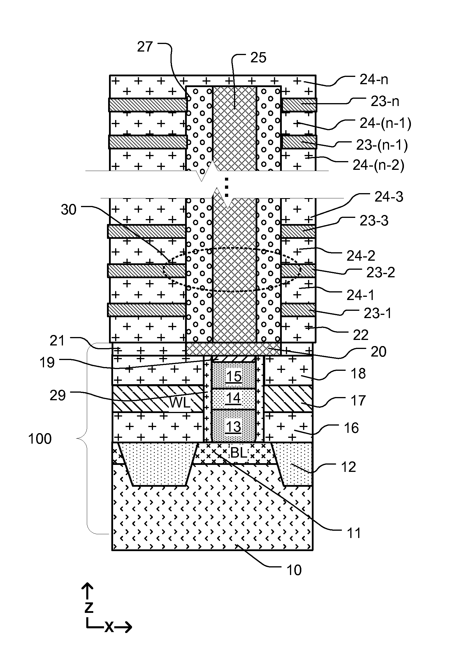
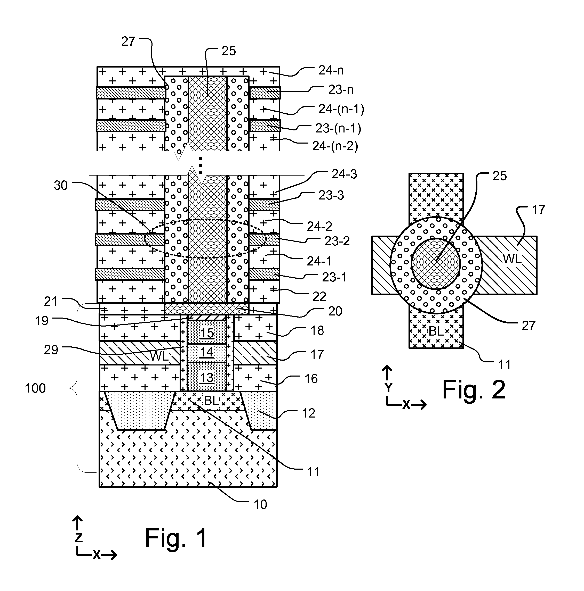
[0027]FIG. 1 illustrates a cross-section of a multi-level memory cell structure. The memory cell is formed on an integrated circuit substrate that in this example includes an access array. The access array comprises access devices which in this example are part of an integrated circuit substrate including a memory cell access layer 100, and arranged to connect to individual pillars (e.g., a pillar including pillar core 25 and liner 27) in an array of pillars.

[0028]The access array in this example includes a semiconductor body 10 with trench isolation structures 12 patterned in lines on the surface. Between the trench isolation structures 12, implants are deposited to form buried diffusion bit lines 11 extending in this view into and out of the page of the drawing. An access device for a pillar core 25 is shown which consists of a vertical FET transistor having a drain 13...


PUM


Abstract

A 3D phase change memory device can store multiple bits per cell represented by a plurality of non-overlapping ranges of resistance all of which are established by different resistance ranges corresponding to respective amorphous phase thickness of the phase change memory material. An array of access devices can underlie a plurality of conductive layers, separated from each other and from the array of access devices by insulating layers. An array of pillars extending through the plurality of conductive layers contact corresponding access devices. The phase memory material is between the pillars and conductive layers. Circuitry is configured to program data in the memory cells using programming pulses having shapes that depend on the resistance range of the cell before programming and the data values to be stored.

Description

RELATED APPLICATIONS[0001]This application claims benefit of U.S. Provisional Patent Application No. 61 / 751,954 filed on 14 Jan. 2013, which application is incorporated by reference as if fully set forth herein.BACKGROUND OF THE INVENTION[0002]1. Field of the Invention[0003]The present invention relates to high density memory devices, and particularly to memory devices in which multiple planes of memory cells are arranged to provide a three-dimensional 3D array.[0004]2. Description of Related Art[0005]As critical dimensions of devices in integrated circuits shrink, designers have been looking to techniques for stacking multiple planes of memory cells to achieve greater storage capacity, and to achieve lower costs per bit. In one technology, a plurality of conductive planes of conductors is intersected by an array of conductive pillars. Individual memory cells are selected by selecting the corresponding pillar and conductive plane. These technologies, however, require a rectifier or ...

Claims


Application Information

Patent Timeline
Patent Type & Authority Applications(United States)
IPC IPC(8): G11C13/00
CPCG11C13/0004G11C11/5678G11C13/0069G11C2213/71H10B63/34H10B63/845H10N70/823H10N70/231H10N70/011H10N70/8828
Inventor LUNG, HSIANG-LAN
Owner MACRONIX INT CO LTD
Why Eureka
Try Eureka