
Semiconductor device including vertical semiconductor element

a technology of semiconductor elements and semiconductor devices, applied in the direction of semiconductor devices, basic electric elements, electrical equipment, etc., to achieve the effect of increasing on-resistan

Inactive Publication Date: 2014-07-24
DENSO CORP
View PDF4 Cites 23 Cited by
  • Summary
  • Abstract
  • Description
  • Claims
  • Application Information

AI Technical Summary

Benefits of technology

The present invention aims to prevent an increase in on-resistance in a semiconductor device that includes a vertical semiconductor element with a super junction structure. The invention achieves this by forming a second trench that is deeper than a first trench, which improves avalanche resistance and restricts the increase in on-resistance.

Problems solved by technology

However, in a case where a voltage drop in an extraction path is too large, an avalanche current flows toward an n+ type source region to operate a parasitic bipolar transistor.
However, in a case where the above-described structure is applied to a vertical MOS transistor having a super junction structure, a high-temperature and long-time heat treatment is necessary to diffuse a high-concentration p+ type body layer to be deeper than a trench filled with a gate electrode.

Method used


Image

  • Semiconductor device including vertical semiconductor element
  • Semiconductor device including vertical semiconductor element
  • Semiconductor device including vertical semiconductor element

Examples


first embodiment

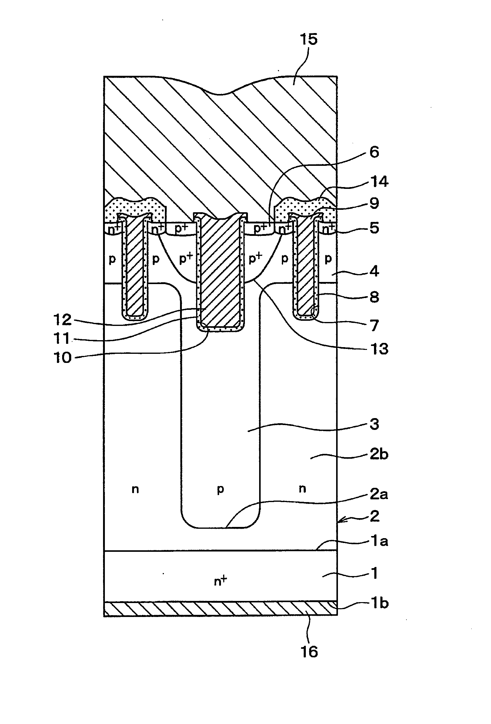
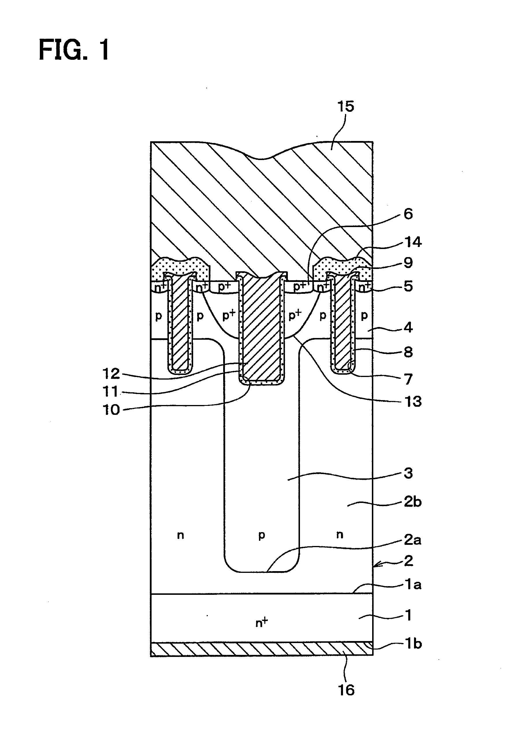
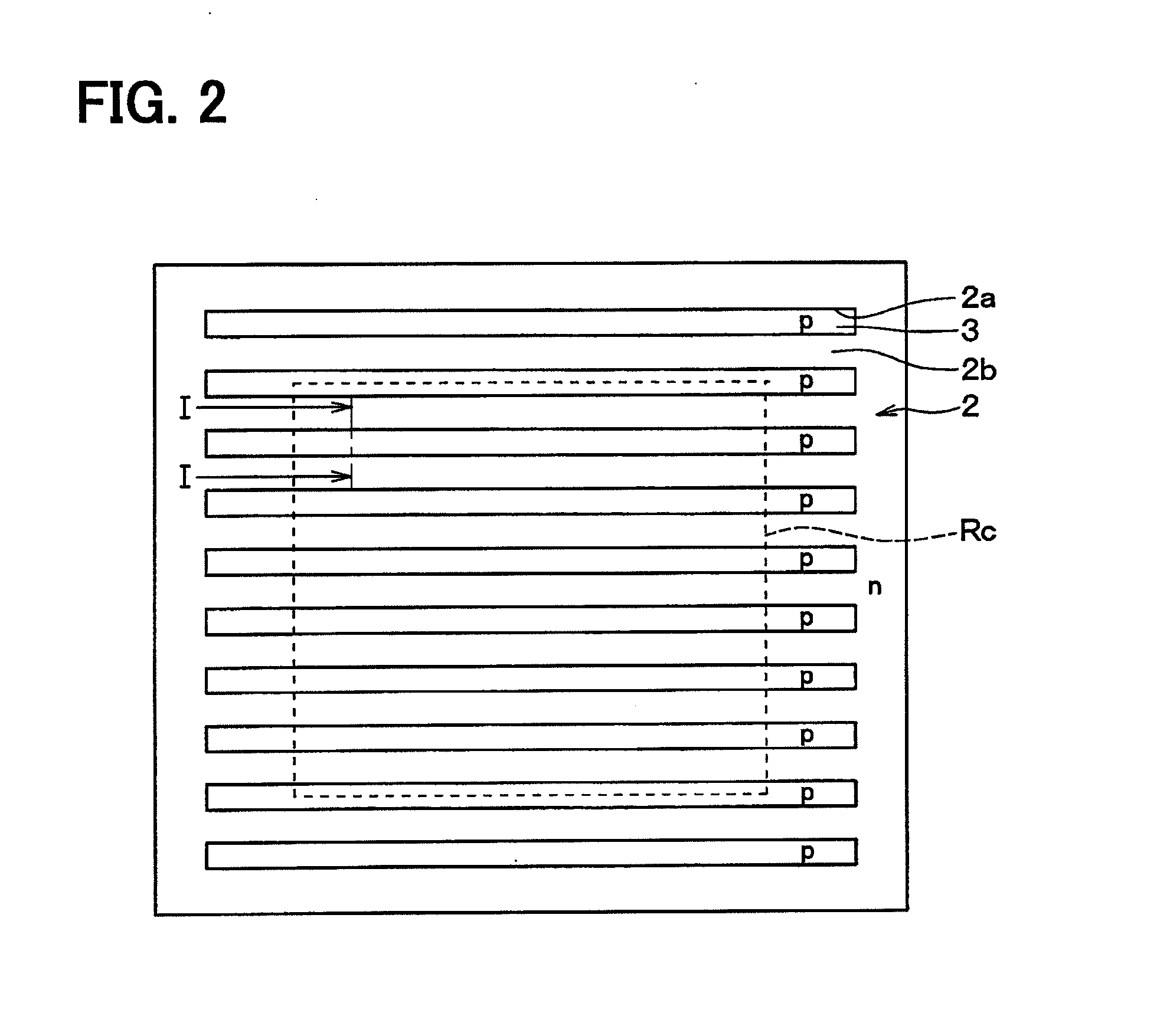
[0029]A first embodiment of the present disclosure will be described. In the present embodiment, a semiconductor device that includes a vertical MOS transistor as a vertical semiconductor element will be described as an example. FIG. 1 is a cross-sectional view illustrating a cell region Rc of a semiconductor device including a vertical MOS transistor according to the present embodiment. FIG. 2 is a diagram illustrating a layout of the semiconductor device illustrated in FIG. 1. FIG. 1 corresponds to a cross-sectional view taken along line I-I in FIG. 2.

[0030]In the semiconductor device according to the present embodiment illustrated in FIG. 1, an inverted vertical MOS transistor having a trench gate structure is provided as a vertical MOS transistor. As illustrated in FIG. 1, the vertical MOS transistor is formed using an n+ type substrate 1 made of single crystal semiconductor such as single crystal silicon. In the n+ type substrate 1, one surface is referred to as a main surface ...

second embodiment

[0050]A second embodiment of the present disclosure will be described. In the present embodiment, a configuration of the super junction structure is changed with respect to the first embodiment, and the other part is similar to the first embodiment. Thus, only a part different from the first embodiment will be described.

[0051]FIG. 6 is a cross-sectional view illustrating a cell region Rc of the semiconductor device including the vertical MOS transistor according to the present embodiment. As illustrated in FIG. 6, in the present embodiment, the dummy gate structure is formed at the positions where the n type regions 2b are formed. Specifically, the longitudinal directions of the first trenches 7 and the second trenches 10 are set to be the same direction as the longitudinal directions of the n type region 2b and the p type regions 3. The first trenches 7 are disposed in every other n type regions 2b, and the second trenches 10 are formed at parts of the n type regions 2b in which th...

third embodiment

[0053]A third embodiment of the present disclosure will be described. In the present embodiment, a configuration of the super junction structure is changed with respect to the first embodiment, and the other part is similar to the first embodiment. Thus, only a part different from the first embodiment will be described.

[0054]FIG. 7(a) and FIG. 7(b) are cross-sectional views illustrating a cell region Rc of the semiconductor device including the vertical MOS transistor according to the present embodiment. FIG. 8 is a diagram illustrating a layout of the semiconductor device illustrated in FIG. 7. FIG. 7(a) and FIG. 7(b) respectively correspond to cross-sectional view taken along lines VIIA-VIIIA, VIIB-VIIB in FIG. 8.

[0055]As illustrated in FIG. 7(a), (b) and FIG. 8, in the present embodiment, the longitudinal directions of the first trenches 7 and the second trenches 10 are set to intersect with the longitudinal directions of the n type regions 2b and the p type regions 3 so that the...


PUM


Abstract

A semiconductor device including a vertical semiconductor element has a trench gate structure and a dummy gate structure. The trench gate structure includes a first trench that penetrates a first impurity region and a base region to reach a first conductivity-type region in a super junction structure. The dummy gate structure includes a second trench that penetrates the base region reach the super junction structure and is formed to be deeper than the first trench.

Description

CROSS REFERENCE TO RELATED APPLICATION[0001]The present disclosure is based on Japanese Patent Application No. 2011-210676 filed on Sep. 27, 2011 and Japanese Patent Application No. 2012-161523 filed on Jul. 20, 2012, the disclosures of which are incorporated herein by reference.TECHNICAL FIELD[0002]The present disclosure relates to a semiconductor device including a vertical semiconductor element.BACKGROUND ART[0003]In a semiconductor device including a vertical MOS transistor, holes are normally extracted from a p type base region. However, in a case where a voltage drop in an extraction path is too large, an avalanche current flows toward an n+ type source region to operate a parasitic bipolar transistor. Thus, an avalanche resistance is reduced. In order to improve the avalanche resistance, it is necessary not to operate the parasitic bipolar transistor formed by the n+ type source region, the p type base region, and an n− type drift layer.[0004]In order to achieve that, convent...

Claims


Application Information

Patent Timeline
IPC IPC(8): H01L29/10H01L29/66H01L29/78
CPCH01L29/1045H01L29/66734H01L29/7813H01L29/0634H01L29/407H01L29/41766H01L29/1095
Inventor KAGATA, YUMAAKAGI, NOZOMU
Owner DENSO CORP
Learn More