Thin film semiconductor device, organic light-emitting display device, and method of manufacturing the thin film semiconductor device

Active Publication Date: 2014-08-14
SAMSUNG DISPLAY CO LTD
View PDF2 Cites 42 Cited by
  • Summary
  • Abstract
  • Description
  • Claims
  • Application Information

AI Technical Summary

Benefits of technology

[0008]The present invention provides a thin film semiconductor device such as an organic light-emitting display device, and a method of manufacturing the thin film semiconductor devi

Problems solved by technology

The strong electric field causes a short channel effect or a hot electron effect, su

Method used


Image

  • Thin film semiconductor device, organic light-emitting display device, and method of manufacturing the thin film semiconductor device
  • Thin film semiconductor device, organic light-emitting display device, and method of manufacturing the thin film semiconductor device
  • Thin film semiconductor device, organic light-emitting display device, and method of manufacturing the thin film semiconductor device

Examples


Example

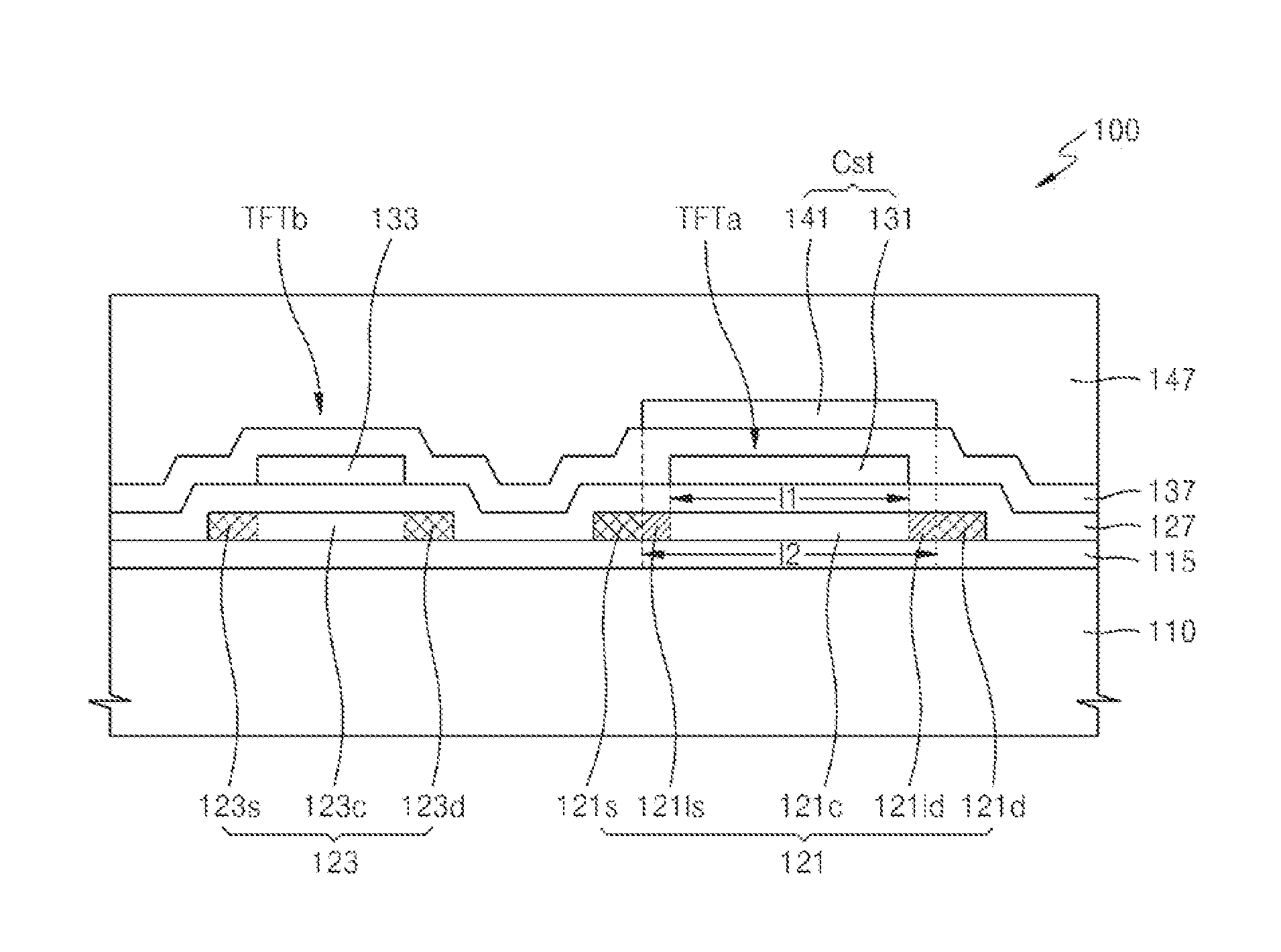
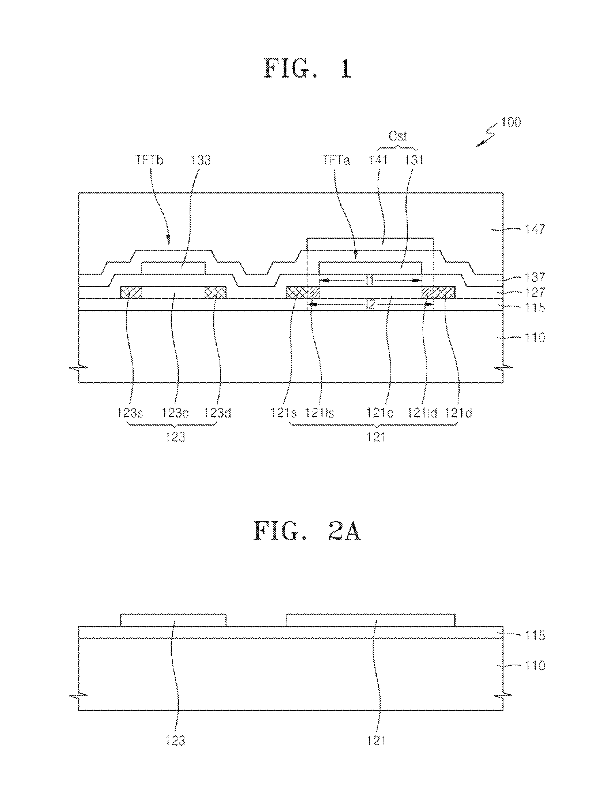
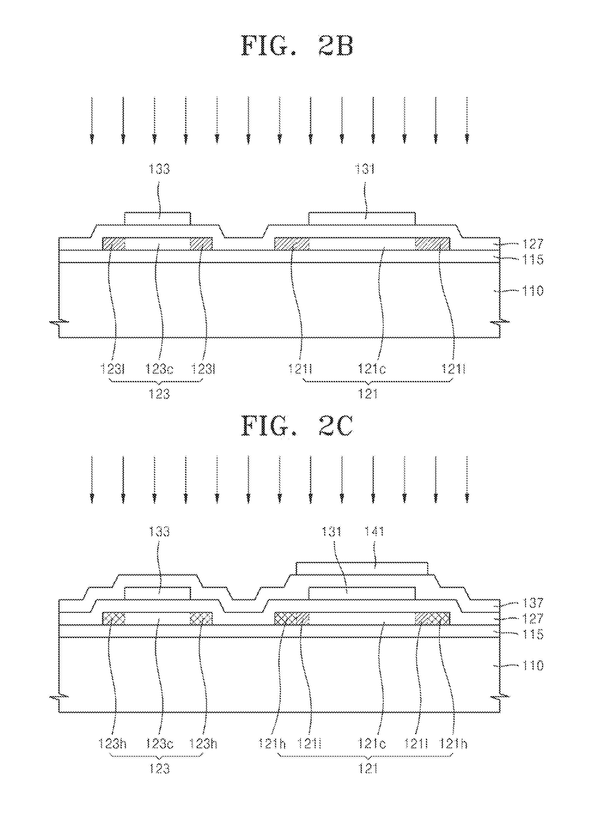
[0038]The present invention will now be described more fully with reference to the accompanying drawings, in which exemplary embodiments of the invention are shown. The invention may, however, be embodied in many different forms, and should not be construed as being limited to the embodiments set forth herein. Thus, the invention may include all revisions, equivalents, or substitutions which are included in the concept and the technical scope related to the invention.

[0039]Like reference numerals in the drawings denote like elements. In the drawings, the dimension of structures may be exaggerated for clarity.

[0040]Furthermore, all examples and conditional language recited herein are to be construed as being without limitation to such specifically recited examples and conditions. Throughout the specification, a singular form may include plural forms, unless there is a particular description contrary thereto. Also, terms such as “comprise” or “comprising” are used to specify existence...


PUM


Abstract

Provided is a thin film semiconductor device such as an organic light-emitting display which includes a thin film transistor (TFT) having a lightly doped region. The thin film semiconductor includes a substrate, a first active pattern, a first lower conductive pattern, and a first upper conductive pattern. The first active pattern is disposed on the substrate and includes a channel region, a lightly doped region, and a heavily doped region. The first lower conductive pattern is disposed on the first active pattern and covers the channel region. The first upper conductive pattern is disposed on the first lower conductive pattern and covers the channel region and the lightly doped region.

Description

CLAIM OF PRIORITY[0001]This U.S. non-provisional patent application claims priority under 35 U.S.C. §119 of Korean Patent Application No. 10-2013-0016052, filed on Feb. 14, 2013, the contents of which are hereby incorporated by reference in its entirety.BACKGROUND OF THE INVENTION[0002]1. Field of the Invention[0003]Embodiments of the present invention generally relates to a thin film semiconductor device such as an organic light-emitting display device, and more particularly, to a thin film semiconductor device such as an organic light-emitting display which includes a thin film transistor (TFT) having improved electrical characteristics.[0004]2. Description of the Related Art[0005]Compared to a semiconductor device using a semiconductor substrate, when a thin film transistor (TFT) is formed by using a semiconductor thin film formed on a glass substrate, manufacturing costs may be reduced and a process for a large area may be easily performed, so that a thin film semiconductor devi...

Claims


Application Information

Patent Timeline
IPC IPC(8): H01L51/52H01L29/786
CPCH01L29/78672H01L2227/323H01L27/3265H01L27/3262H01L29/78621H01L27/1255H10K59/1213H10K59/1216H10K59/1201H01L29/66757H01L29/78645H01L29/78675
Inventor ZHAN, ZHI-FENG
Owner SAMSUNG DISPLAY CO LTD
Why Eureka
Try Eureka