
Array substrate for liquid crystal display device and method of fabricating the same

a liquid crystal display and substrate technology, applied in non-linear optics, instruments, optics, etc., can solve the problems of difficult to implement a tft using hydrogenated amorphous silicon in a driving circuit, unstable tft, and special deformation of electrical characteristics of hydrogenated amorphous silicon, so as to reduce the number of mask processes, reduce production costs and defect rates, and reduce the effect of mask process number

Inactive Publication Date: 2009-01-06
LG DISPLAY CO LTD
View PDF1 Cites 2 Cited by
  • Summary
  • Abstract
  • Description
  • Claims
  • Application Information

AI Technical Summary

Benefits of technology

[0051]An advantage of the present invention is to provide an array substrate for an LCD device and a method of fabricating the same by using a reduced number of mask processes.
[0052]Another advantage of the present invention is to provide an array substrate for an LCD device and a method of fabricating the same that has an improved product yield because mask processes, production costs and defect rates are reduced.

Problems solved by technology

However, because the atomic arrangement of the hydrogenated amorphous silicon is disordered, weak silicon-silicon (Si—Si) bonds and dangling bonds exist in the hydrogenated amorphous silicon.
As a result, this metastability makes the TFT unstable.
Electrical characteristics of hydrogenated amorphous silicon are especially degraded due to light irradiation.
Furthermore, it is difficult to implement a TFT using hydrogenated amorphous silicon in a driving circuit because electric characteristics are degraded.
These degraded electric characteristics include a relatively low field effect mobility and poor reliability.
As explained above, the fabricating method of the array substrate according to the related art includes at least nine mask processes, thereby deteriorating the product yield by increasing product costs and product time.
Further, because at least nine mask processes may be performed, the rate of defects may increase.

Method used


Image

  • Array substrate for liquid crystal display device and method of fabricating the same
  • Array substrate for liquid crystal display device and method of fabricating the same
  • Array substrate for liquid crystal display device and method of fabricating the same

Examples


Embodiment Construction

[0071]Reference will now be made in detail to embodiments of the present invention, examples of which are illustrated in the accompanying drawings. Wherever possible, similar reference numbers will be used to refer to the same or similar parts.

[0072]FIG. 7 is a schematic plan view showing a display area of an array substrate for an LCD device according to an embodiment of the present invention.

[0073]In FIG. 7, a gate line “GL” and a data line “DL” cross each other to define a pixel electrode “P.” A switching thin film transistor “Ts” is connected to the gate line “GL” and the data line “DL.” A pixel electrode 172 is connected to the switching thin film transistor “Ts.” For example, the switching thin film transistor “Ts” includes a gate electrode 148, a semiconductor layer 116, a source electrode 164a and a drain electrode 164b. The semiconductor layer 116 may include polysilicon material.

[0074]Further, a storage capacitor “Cst” includes first, second and third storage electrodes 12...


PUM

PropertyMeasurementUnit
areaaaaaaaaaaa
concentrationaaaaaaaaaa
conductiveaaaaaaaaaa

Abstract

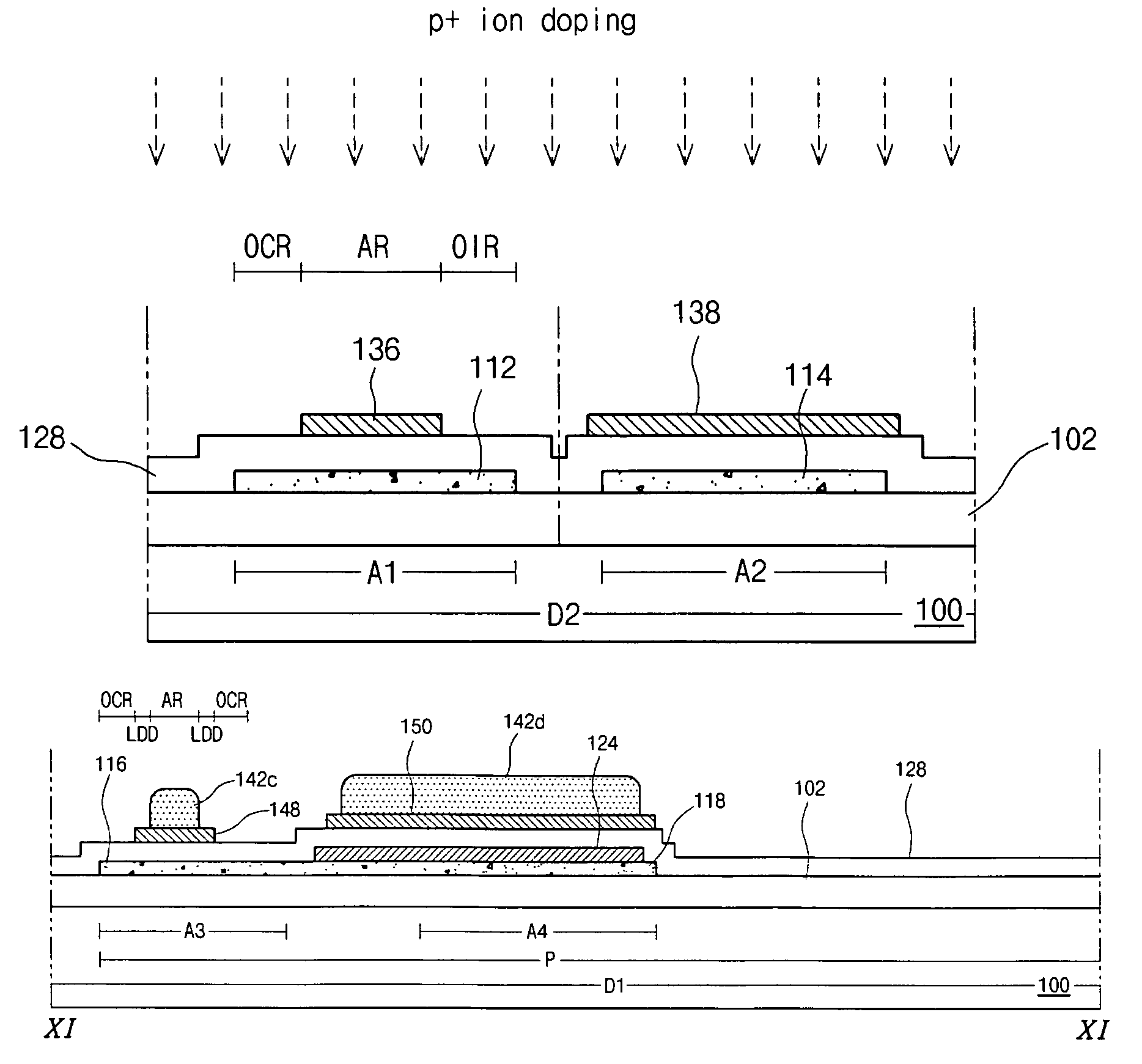
An array substrate for an LCD device and a method of fabricating the same are disclosed. The array substrate includes: a substrate defining a display area and a non-display area; an n-type driving TFT and a p-type driving TFT in the non-display area; a switching TFT in the display region; a storage capacitor in the display region, the storage capacitor including first to third storage layers sequentially layered with intervening insulating layers, wherein the first storage layer contacts a first semiconductor layer under the first storage layer; and a pixel electrode in the display region, the pixel electrode connected to the switching TFT.

Description

[0001]This application claims the benefit of Korean Patent Application No. 10-2005-0106837, filed on Nov. 9, 2005, which is hereby incorporated by reference for all purposes as if fully set forth herein.BACKGROUND OF THE INVENTION[0002]1. Field of the Invention[0003]The present invention relates to a liquid crystal display (LCD) device, and more particularly, to an array substrate for an LCD device and a method of fabricating the same.[0004]2. Discussion of the Related Art[0005]Flat panel display (FPD) devices having high portability and low power consumption have been the subject of recent research and development. Liquid crystal display (LCD) devices are a type of FPD devices and are commonly used as monitors for notebook and desktop computers because of their ability to display high-resolution images, wide ranges of different colors, and moving images.[0006]In most cases, an LCD device includes a color filter substrate and an array substrate separated from each other and having a...

Claims


Application Information

Patent Timeline
Patent Type & Authority Patents(United States)
IPC IPC(8): H01L29/04G02F1/1368H01L21/336H01L29/786
CPCH01L27/1255H01L27/1288G02F1/13454G02F1/136213G02F1/136
Inventor LEE, SEOK-WOOPARK, YONG-IN
Owner LG DISPLAY CO LTD
Learn More