Patterning method and method of forming memory device

a memory device and patterning technology, applied in the manufacturing of semiconductor/solid-state devices, basic electric elements, electric devices, etc., can solve the problem of inability to accurately control to the target value, and achieve the effect of improving cdu

Active Publication Date: 2014-09-04
WINBOND ELECTRONICS CORP
View PDF12 Cites 170 Cited by
  • Summary
  • Abstract
  • Description
  • Claims
  • Application Information

AI Technical Summary

Benefits of technology

[0037]In view of the above, in the patterning method and in the method of forming a memory device of the invention, the select gates of dense areas are removed from the original photomask data. Next, multiple dummy patterns with the same line-width and the same pitch are added into the removed area and an open area adjacent to the dense areas, so as to form a modified photomask data. Since the dummy patterns are added into the open area t

Problems solved by technology

However, when word lines of a memory are defined with the current techniques, the line-width of the word lines adjacent to

Method used


Image

  • Patterning method and method of forming memory device
  • Patterning method and method of forming memory device
  • Patterning method and method of forming memory device

Examples


Embodiment Construction

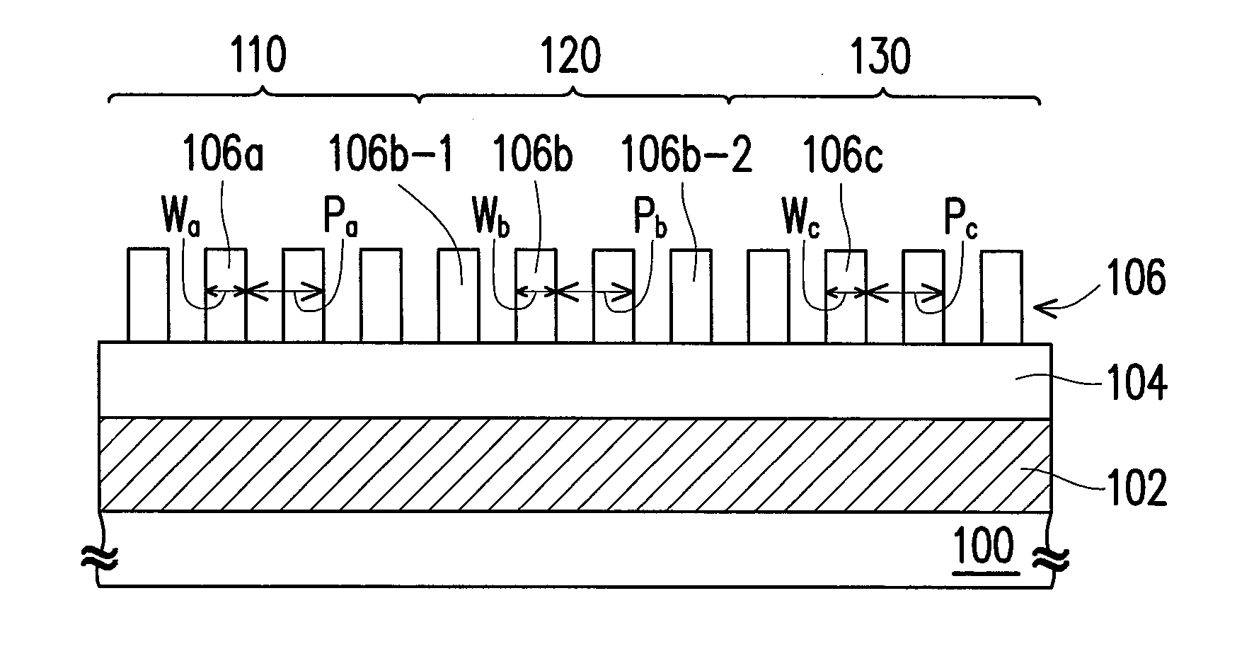
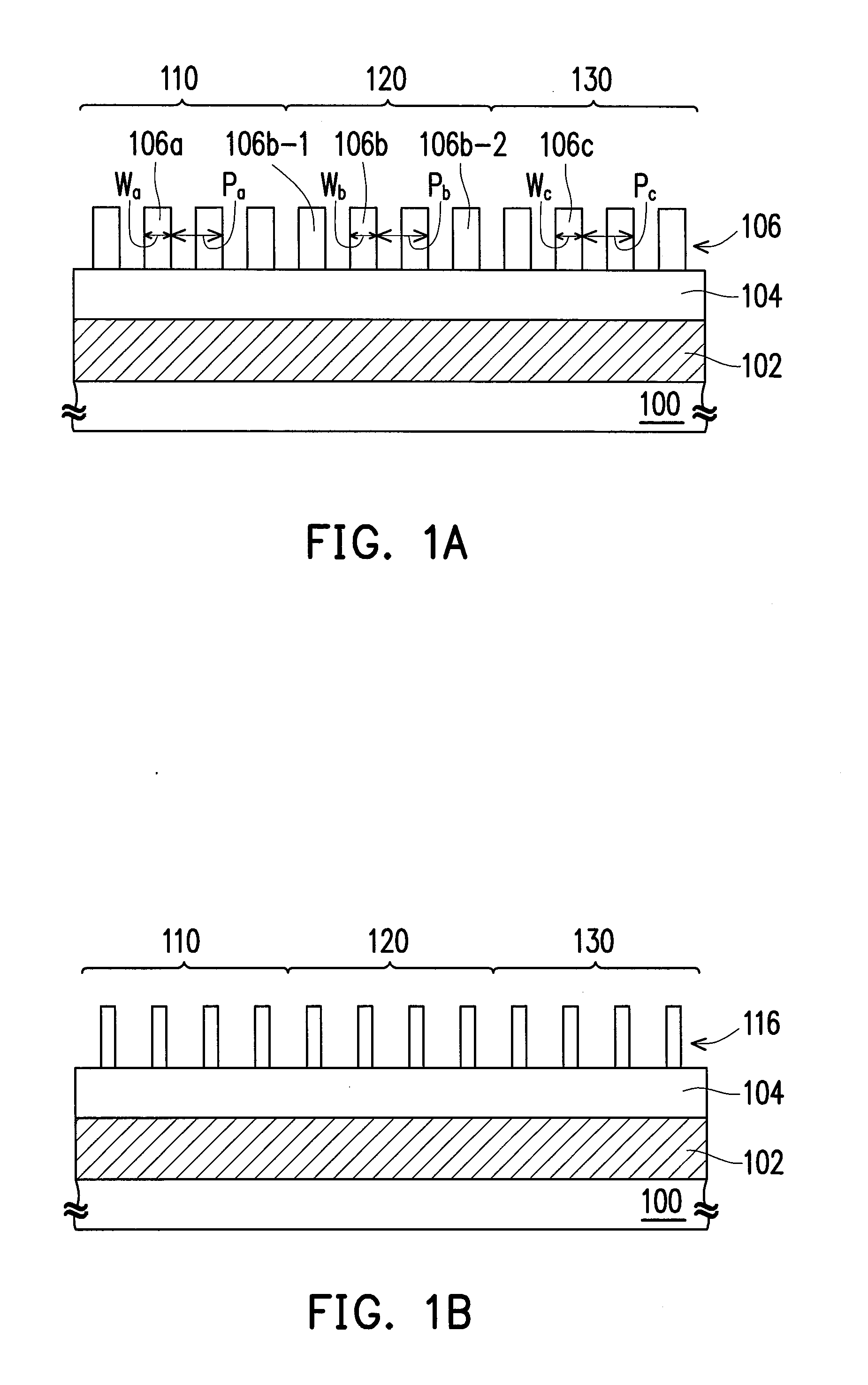
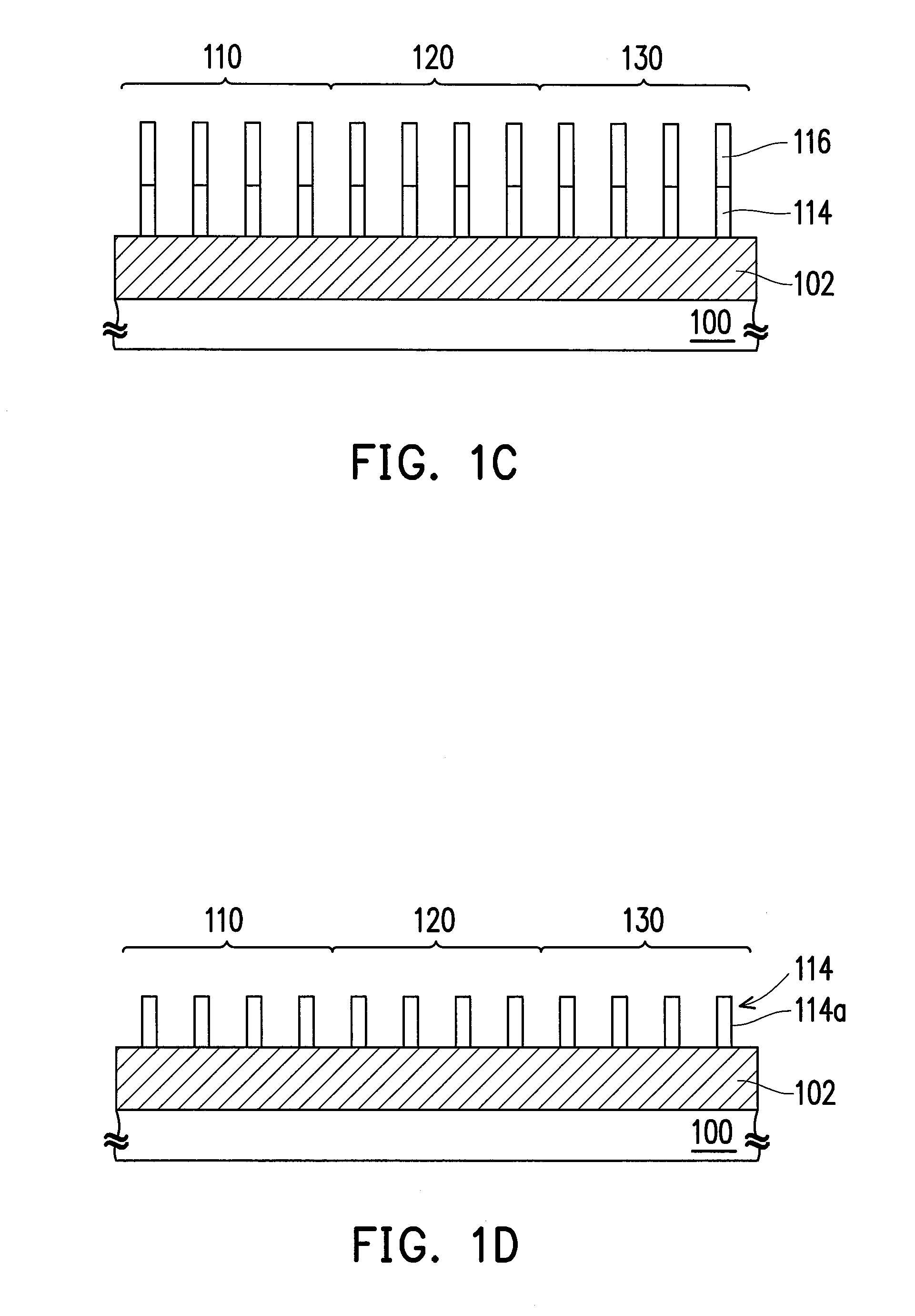
[0044]FIG. 1A to FIG. 1M are cross-sectional diagrams showing a patterning method according to an embodiment of the invention.

[0045]Referring to FIG. 1A, a substrate 100 is provided. The substrate 100 has a first area 110, a second area 120 and a third area 130. The second area 120 is located between the first area 110 and the third area 130. The substrate 100 is, for example, a silicon substrate or a suitable semiconductor substrate. In an embodiment, both the first area 110 and the third area 130 can be cell areas of a memory, while the second area 120 can be a peripheral area or an open area of the memory. Next, a target layer 102 and a sacrificial layer 104 are sequentially formed on the substrate 100. The target layer 102 is, for example, a single layer or a stacked layer. In an embodiment, when the target layer 102 is a single layer, the material thereof can be doped polysilicon. In another embodiment, when the target layer 102 is a stacked layer including a dielectric layer a...


PUM


Abstract

A method of forming memory device is provided. A substrate having at least two cell areas and at least one peripheral area between the cell areas is provided. A target layer, a sacrificed layer and a first mask layer having first mask patterns in the cell areas and second mask patterns in the peripheral area are sequentially formed on the substrate. Sacrificed layer is partially removed to form sacrificed patterns by using the first mask layer as a mask. Spacers are formed on sidewalls of the sacrificed patterns. The sacrificed patterns and at least the spacers in the peripheral area are removed. A second mask layer is formed in the cell areas. Target layer is partially removed, using the second mask layer and remaining spacers as a mask, to form word lines in the cell areas and select gates in a portion of cell areas adjacent to the peripheral area.

Description

CROSS-REFERENCE TO RELATED APPLICATION[0001]This application claims the priority benefit of Taiwan application serial no. 102107353, filed on Mar. 1, 2013. The entirety of the above-mentioned patent application is hereby incorporated by reference herein and made a part of this specification.BACKGROUND OF THE INVENTION[0002]1. Field of the Invention[0003]The invention generally relates to a semiconductor process and a method of forming a semiconductor device, and more particularly to a patterning method and a method of forming a memory device.[0004]2. Description of Related Art[0005]A non-volatile memory provides the properties of multiple writing, reading and erasing operations of data, and is able to retain the stored information even when the electrical power is off. As a result, the non-volatile memory is widely used in personal computers and consumer electronic products. As the level of integration of a non-volatile memory is getting higher, the critical dimension (CD) thereof i...

Claims


Application Information

Patent Timeline
IPC IPC(8): H01L21/306
CPCH01L21/306H01L21/0274H01L21/0337H01L21/32139H10B41/41H10B41/42H10B43/40H10B41/46
Inventor TSAI, JEN-HSIANG
Owner WINBOND ELECTRONICS CORP
Why Eureka
Try Eureka