

Liquid crystal display
a liquid crystal display and display device technology, applied in non-linear optics, instruments, optics, etc., can solve the problems of unsatisfactory degree but in some respects, non-uniform alignment control force applied to liquid crystal molecules within pixel boundaries, and unintentional distribution of response speed, so as to reduce the viewing angle dependence of the characteristic of a va mode liquid crystal display devi
- Summary
- Abstract
- Description
- Claims
- Application Information
AI Technical Summary
Benefits of technology
Problems solved by technology
Method used
Image

Examples
embodiment 1
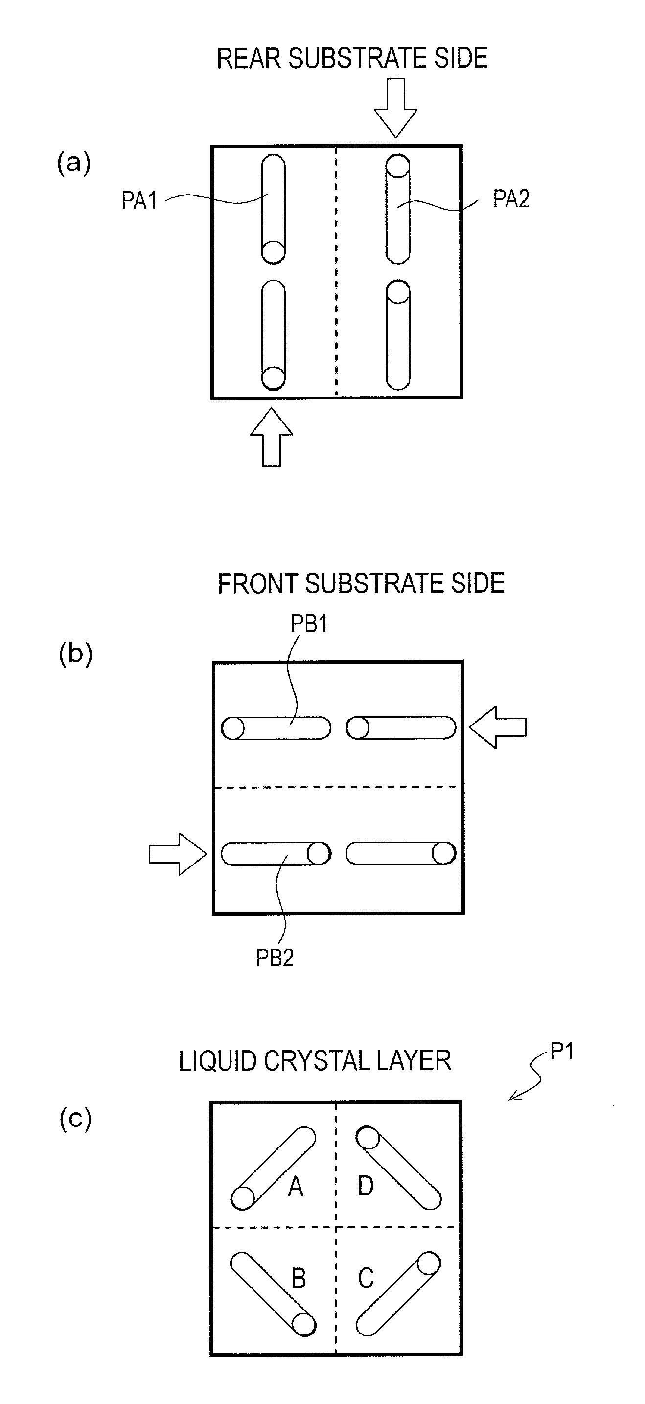
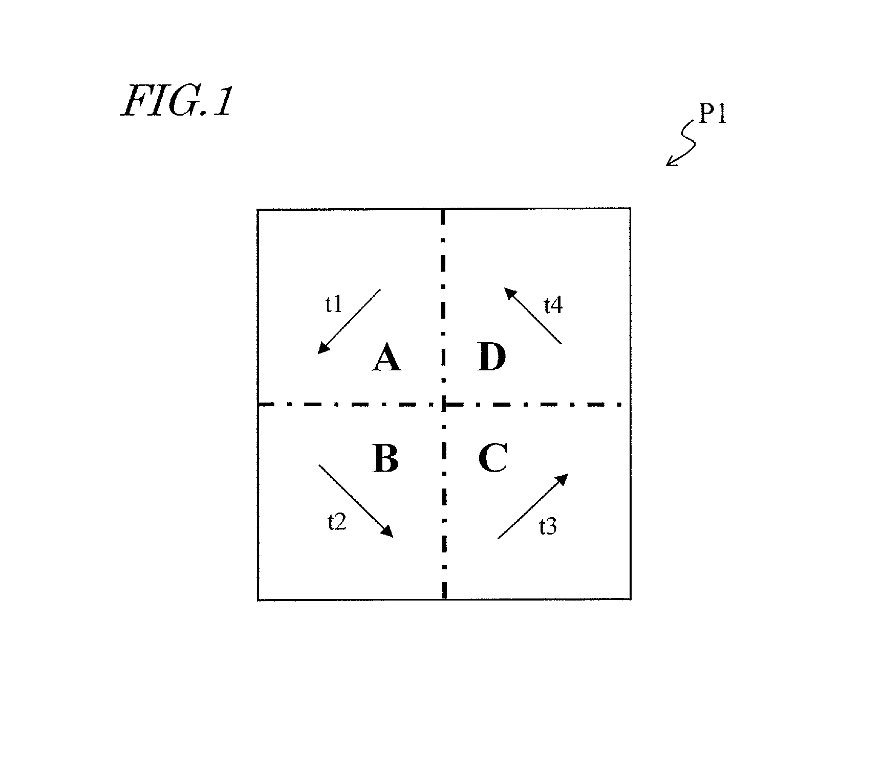
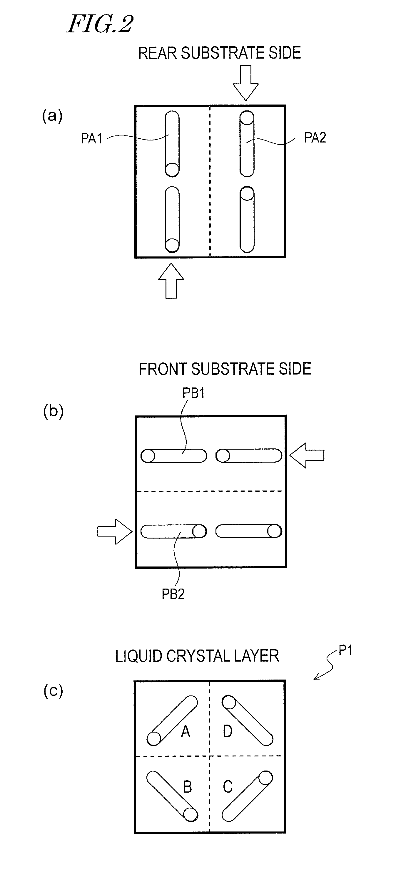
[0132]FIGS. 6 and 7 illustrate a liquid crystal display device 100 as a first embodiment of the present invention. The liquid crystal display device 100 includes a plurality of pixel regions which are arranged in a matrix pattern. FIG. 6 is a plan view schematically illustrating one of those multiple pixel regions of the liquid crystal display device 100, and FIG. 7 is a cross-sectional view of the device as viewed on the plane 7A-7A′ shown in FIG. 6.
[0133]As shown in FIG. 7, this liquid crystal display device 100 includes a liquid crystal layer 30 and an active-matrix substrate 10 and a counter substrate 20 which face each other with the liquid crystal layer 30 interposed between them. The liquid crystal display device 100 further includes pixel electrodes 11, a counter electrode 21, and two photo-alignment films 12 and 22.
[0134]The liquid crystal layer 30 is a vertical alignment liquid crystal layer and includes liquid crystal molecules (not shown in FIG. 7) with negative dielectr...
embodiment 2
[0168]FIGS. 11 and 12 illustrate a liquid crystal display device 200 as a second embodiment of the present invention. FIG. 11 is a plan view schematically illustrating a single pixel region of the liquid crystal display device 200, and FIG. 12 is a cross-sectional view of the device as viewed on the plane 12A-12A′ shown in FIG. 11. The following description of this second embodiment will be focused on only the differences of this liquid crystal display device 200 from the liquid crystal display device 100 of the first embodiment. Also, on the drawings, any component having substantially the same function as its counterpart of the liquid crystal display device 100 is identified by the same reference numeral and description thereof will be omitted herein (and the same statement will apply to the rest of the description of embodiments).
[0169]The active-matrix substrate 10 of this liquid crystal display device 200 further includes another electrode 15 which is arranged under the pixel e...
embodiment 3
[0180]FIG. 15 is a plan view schematically illustrating a single pixel region of a liquid crystal display device 300 as a third embodiment of the present invention.
[0181]In the liquid crystal display device 300 of this embodiment, the relative positions of the slit cut regions 11R1 and slit uncut regions 11R2 in the pixel electrode 11 are different from in the liquid crystal display device 100 of the first embodiment.
[0182]Specifically, according to this embodiment, in the regions of the pixel electrode 11 allocated to the liquid crystal domains A and D, the slit cut regions 11R1 form a relatively lower part and the slit uncut regions 11R2 form a relatively upper part as shown in FIG. 15. On the other hand, in the regions of the pixel electrode 11 allocated to the liquid crystal domains B and C, the slit cut regions 11R1 form a relatively upper part and the slit uncut regions 11R2 form a relatively lower part. That is to say, although the slits 11s are arranged in the upper and lowe...
PUM
 Abstract
Description
Claims
Application Information