
Local buried channel dielectric for vertical NAND performance enhancement and vertical scaling

a dielectric and vertical scaling technology, applied in the field of semiconductor fabrication, can solve the problems of serious limitation of achieving the programming operational requirements of an array of vertical nand strings, unavoidable voltage loss mechanism, and deleterious effects

Active Publication Date: 2014-09-18
INTEL CORP
View PDF1 Cites 12 Cited by
  • Summary
  • Abstract
  • Description
  • Claims
  • Application Information

AI Technical Summary

Benefits of technology

The patent text describes techniques for fabricating vertical NAND strings, which can address issues related to conventional planar NAND string architectures. The vertical NAND strings have a unique structure that can result in deleterious effects during programming operations, such as voltage loss and reduced programming speed. The techniques described in the patent text can help to maintain the boosted channel voltage on inhibited pillars and improve programming operational requirements of the array. The patent text also describes various stages of a flow diagram for forming a buried channel dielectric in a channel of a vertical NAND string. Overall, the patent text provides a solution for improving the fabrication and operation of vertical NAND strings.

Problems solved by technology

Vertical NAND strings comprising a polysilicon channel may introduce several deleterious effects into fabrication / operational processes in comparison to conventional planar NAND string architectures having single crystalline silicon channels.
For example, one operational challenge for a vertical NAND string relates to maintaining the boosted channel voltage on inhibited pillars during programming operations.
Localized gap-state defects in the channel material, may introduce a rate-limiting channel-boost voltage-loss mechanism occurring at the edge of the string adjacent to select gate drain on program inhibited strings that potentially poses a serious limitation for achieving programming operational requirements of an array of vertical NAND strings.
The voltage-loss mechanism may be unavoidable when using a non-crystalline channel material (i.e., polysilicon) under standard NAND operation conditions.

Method used


Image

  • Local buried channel dielectric for vertical NAND performance enhancement and vertical scaling
  • Local buried channel dielectric for vertical NAND performance enhancement and vertical scaling
  • Local buried channel dielectric for vertical NAND performance enhancement and vertical scaling

Examples


Embodiment Construction

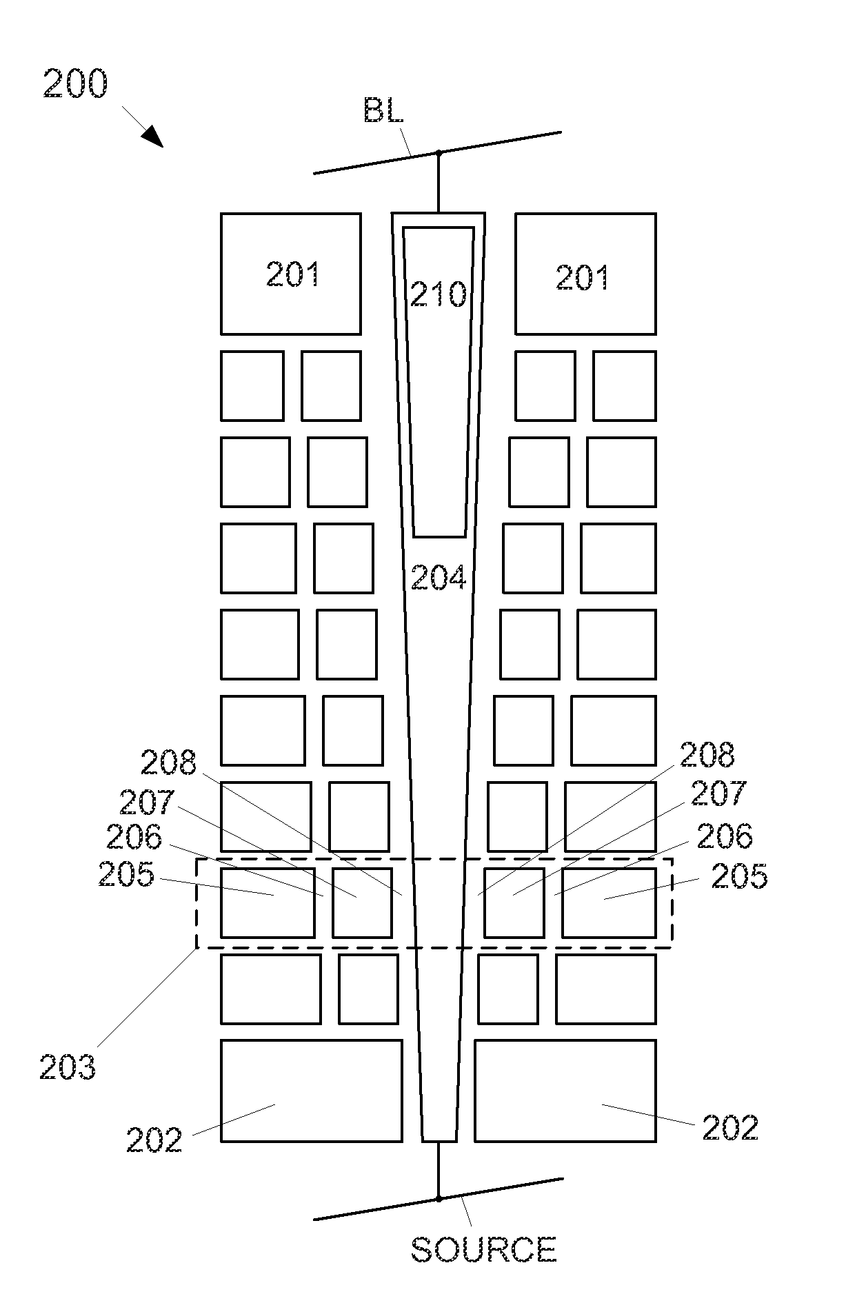
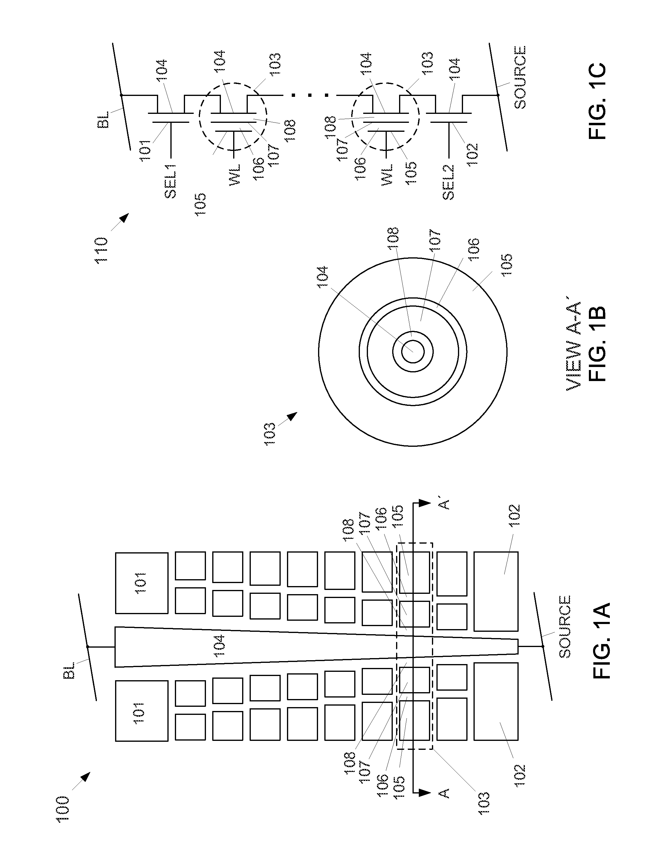
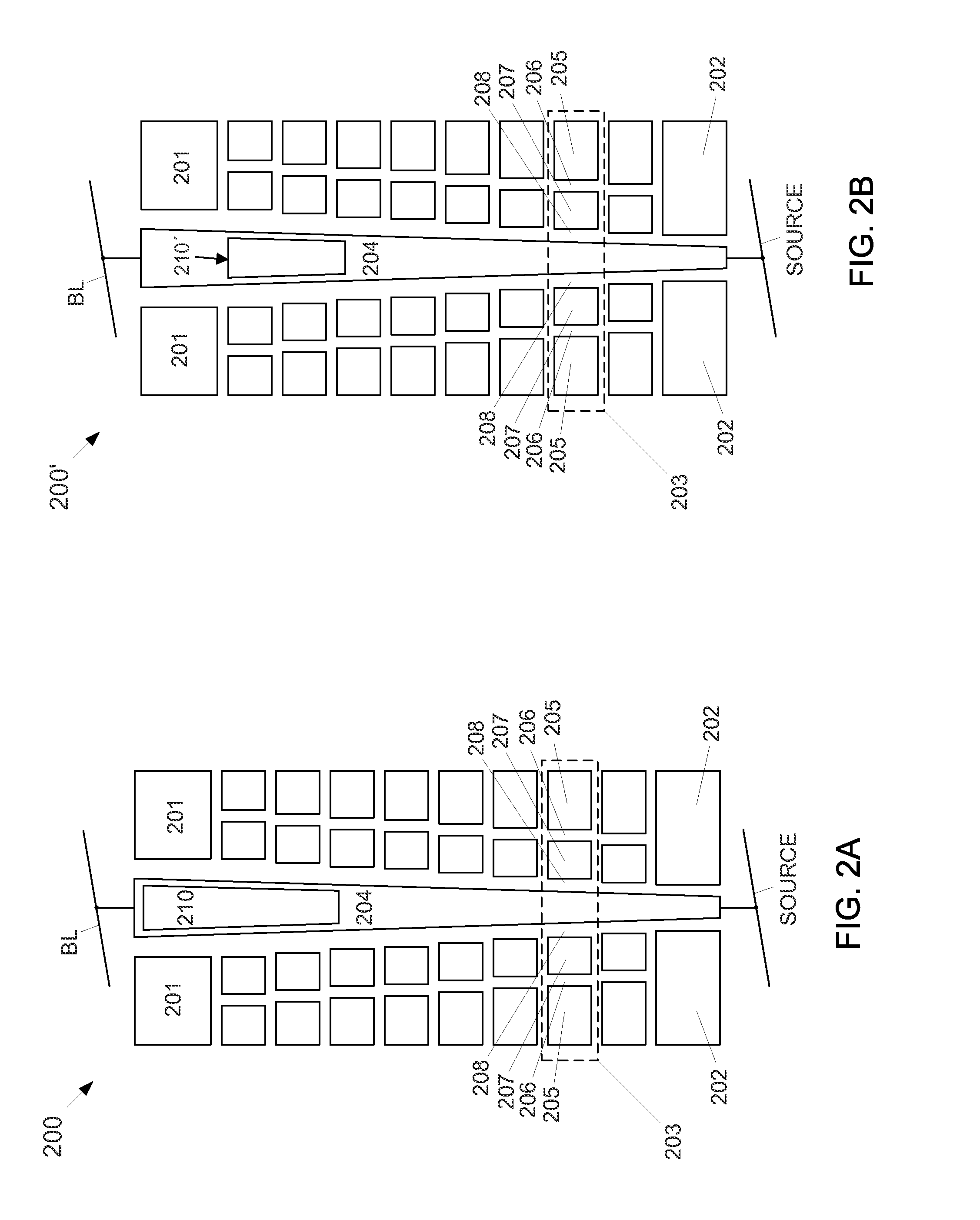
[0023]Embodiments of techniques described herein relate to semiconductor fabrication and, more particularly, to fabricating vertical NAND strings. In the following description, numerous specific details are set forth to provide a thorough understanding of embodiments disclosed herein. One skilled in the relevant art will recognize, however, that the embodiments disclosed herein can be practiced without one or more of the specific details, or with other methods, components, materials, and so forth. In other instances, well-known structures, materials, or operations are not shown or described in detail to avoid obscuring aspects of the specification.

[0024]Reference throughout this specification to “one embodiment” or “an embodiment” means that a particular feature, structure or characteristic described in connection with the embodiment is included in at least one embodiment. Thus, appearances of the phrases “in one embodiment” or “in an embodiment” in various places throughout this sp...


PUM


Abstract

A non-volatile memory device and a method for forming the non-volatile memory device are disclosed. The memory device utilizes a local buried channel dielectric in a NAND string that reduces bulk channel leakage at the edge of the NAND string where the electric field gradient along the direction of the string pillar is at or near a maximum during programming operations. The memory device comprises a channel that is coupled at one end to a bitline and at the other end to a source. A select gate is formed at the end of the channel coupled to the bitline to selectively control conduction between the bitline and the channel. At least one non-volatile memory cell is formed along the length of the channel between the select gate and the second end of the channel. A local dielectric region is formed within the channel at the first end of the channel.

Description

TECHNICAL FIELD[0001]Embodiments of techniques described herein relate to semiconductor fabrication. In particular, the subject matter disclosed herein relates to fabricating vertical NAND strings.BACKGROUND[0002]Vertical NAND strings comprising a polysilicon channel may introduce several deleterious effects into fabrication / operational processes in comparison to conventional planar NAND string architectures having single crystalline silicon channels. For example, one operational challenge for a vertical NAND string relates to maintaining the boosted channel voltage on inhibited pillars during programming operations. Localized gap-state defects in the channel material, may introduce a rate-limiting channel-boost voltage-loss mechanism occurring at the edge of the string adjacent to select gate drain on program inhibited strings that potentially poses a serious limitation for achieving programming operational requirements of an array of vertical NAND strings. The voltage-loss mechani...

Claims


Application Information

Patent Timeline
Patent Type & Authority Applications(United States)
IPC IPC(8): H01L29/66H01L29/788H01L29/792H01L29/78H10B43/27H10B41/27H10B41/35H10B43/35H10B69/00
CPCH01L29/66666H01L29/7827H01L27/11582H01L29/7926H01L27/11556H01L29/7889H10B41/27H10B43/27H10B41/35H10B43/35
Inventor KOVAL, RANDY J.SIMSEK-EGE, FATMA A.
Owner INTEL CORP
Learn More