Display device and method of manufacturing the same
- Summary
- Abstract
- Description
- Claims
- Application Information
AI Technical Summary
Benefits of technology
Problems solved by technology
Method used
Image
Examples
Embodiment Construction
[0038]It will be understood that when an element or layer is referred to as being “on”, “connected to” or “coupled to” another element or layer, it can be directly on, connected or coupled to the other element or layer or intervening elements or layers may be present. Like numbers refer to like elements throughout.
[0039]Hereinafter, exemplary embodiments of the present disclosure will be explained in detail with reference to the accompanying drawings.
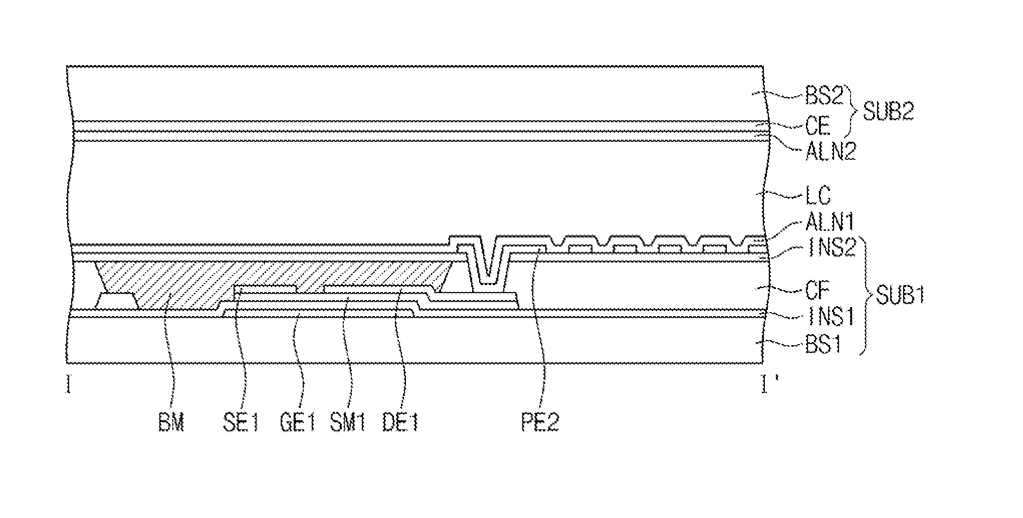
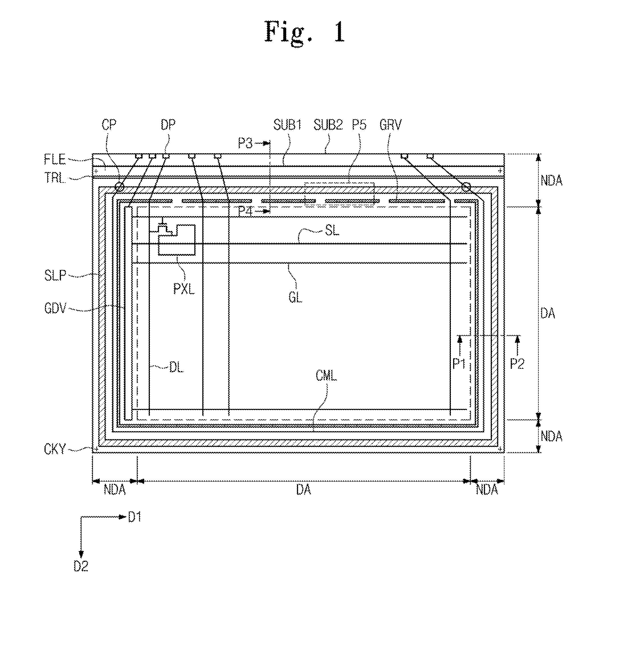
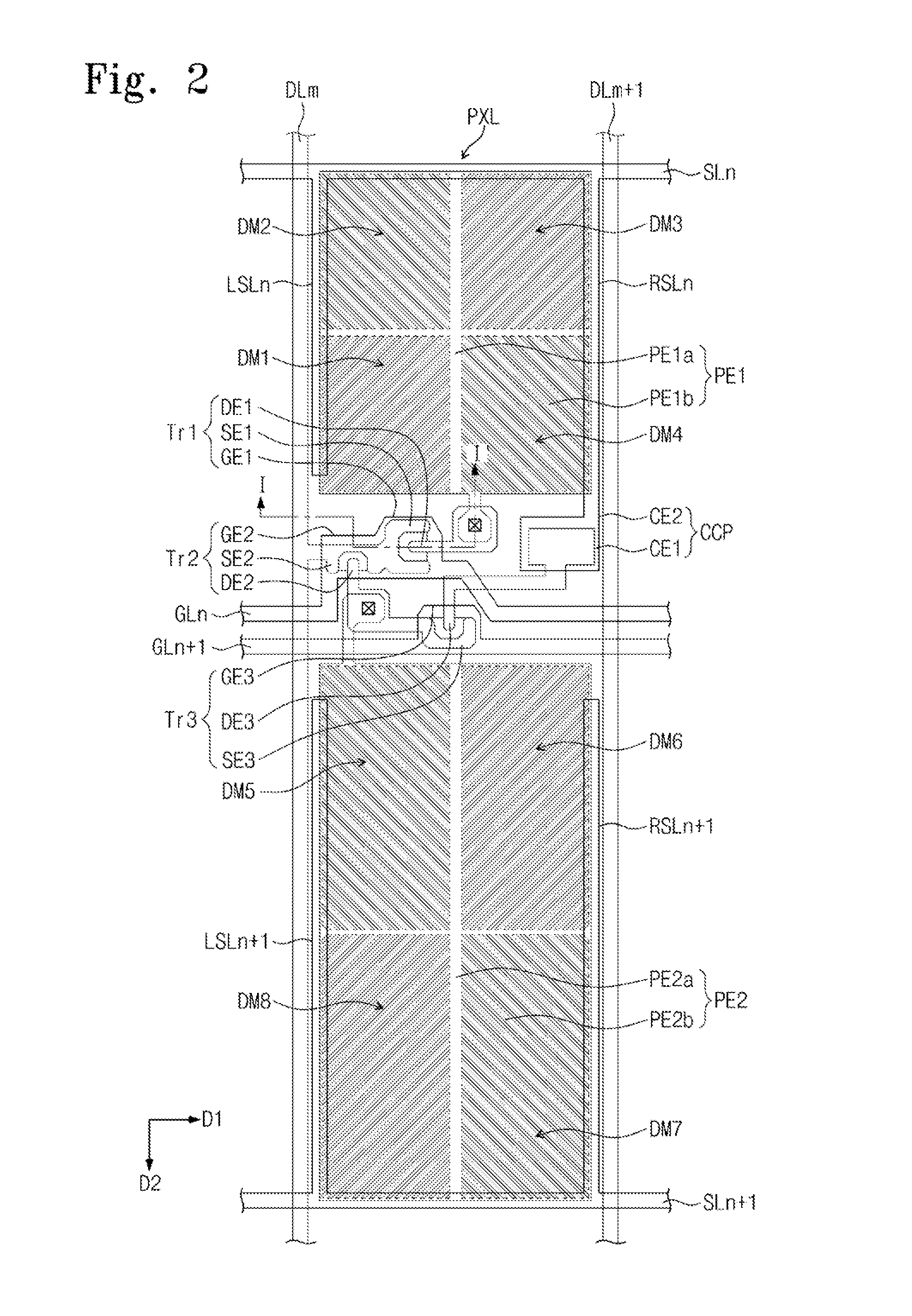
[0040]FIG. 1 is a plan view of a display device according to an exemplary embodiment of the present disclosure, FIG. 2 is a plan view of one pixel of the display device shown in FIG. 1, FIG. 3 is a cross-sectional view taken along a line of FIG. 2, and FIG. 4 is an equivalent circuit diagram of the pixel shown in FIG. 2.
[0041]Referring to FIGS. 1 to 4, a display device has a rectangular shape with a pair of long sides and a pair of short sides. The display device includes a display area DA that includes a plurality of pixels PXL to disp...
PUM
| Property | Measurement | Unit |
|---|---|---|
| Width | aaaaa | aaaaa |
| Distance | aaaaa | aaaaa |
| Shape | aaaaa | aaaaa |
Abstract
Description
Claims
Application Information


