Junction termination structures including guard ring extensions and methods of fabricating electronic devices incorporating same

a technology of junction termination and guard ring, which is applied in the direction of basic electric elements, semiconductor devices, electrical equipment, etc., can solve the problems of long-term reliability problems, high oxide, and adversely affect the breakdown voltage of the devi

Active Publication Date: 2014-10-30
CREE INC
View PDF1 Cites 2 Cited by
  • Summary
  • Abstract
  • Description
  • Claims
  • Application Information

AI Technical Summary

Benefits of technology

[0013]An electronic device according to some embodiments may include a semiconductor layer having a first conductivity type and having a first surface, and a primary junction in the semiconductor layer at the first surface thereof. A lightly doped region is in the semiconductor adjacent the primary junction and has a second conductivity type that is opposite the first conductivity type, and a junction termination structure is in the lightly doped region. The junction termination

Problems solved by technology

Surface effects may cause the depletion region to spread unevenly, which may adversely affect the breakdown voltage of the device.
This leads to very high oxide fields and may result in long-term reliability problems.
Thus, field plate terminations may be unsuitable for use in SiC devices.
Kinoshita et al. report

Method used


Image

  • Junction termination structures including guard ring extensions and methods of fabricating electronic devices incorporating same
  • Junction termination structures including guard ring extensions and methods of fabricating electronic devices incorporating same
  • Junction termination structures including guard ring extensions and methods of fabricating electronic devices incorporating same

Examples


Embodiment Construction

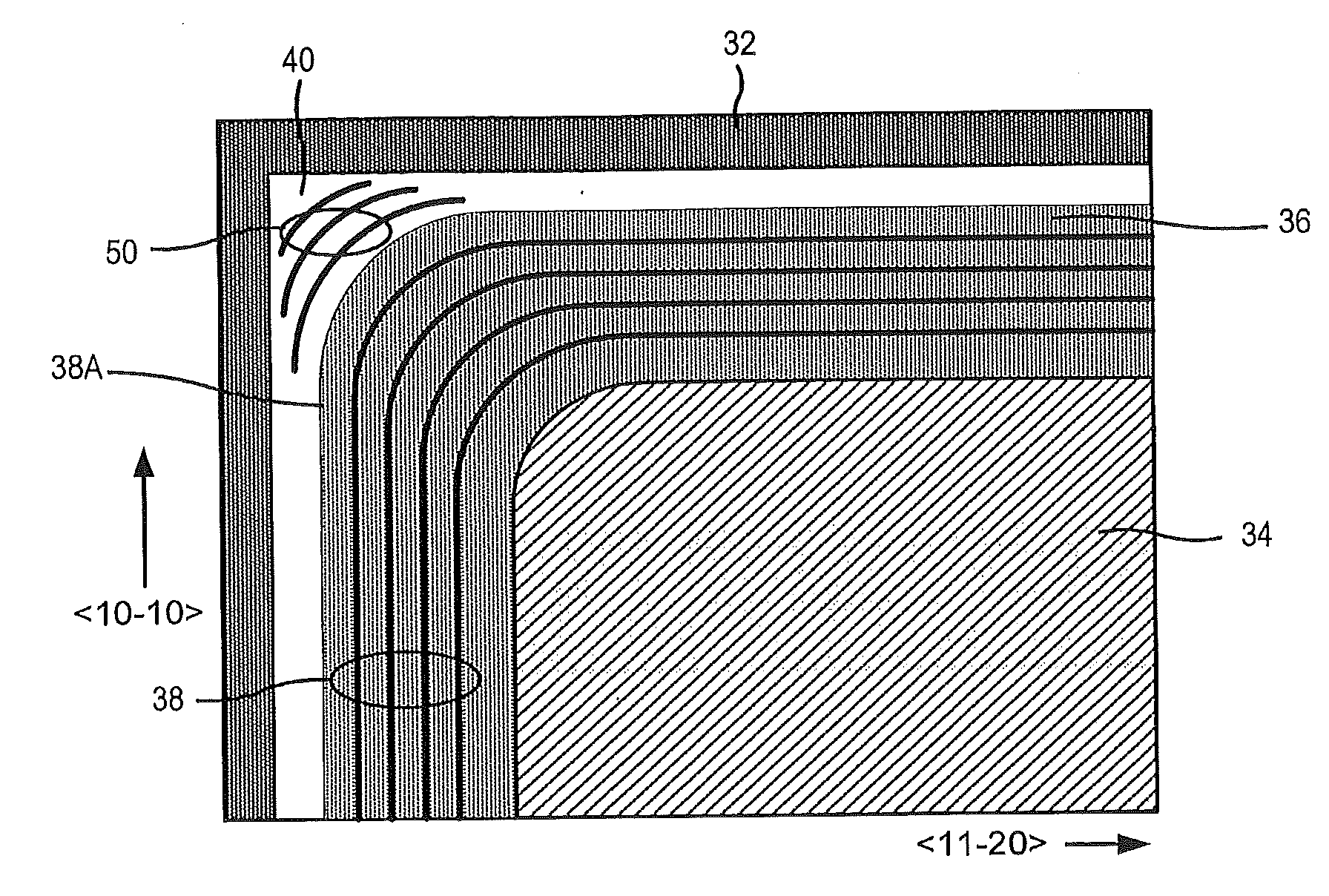
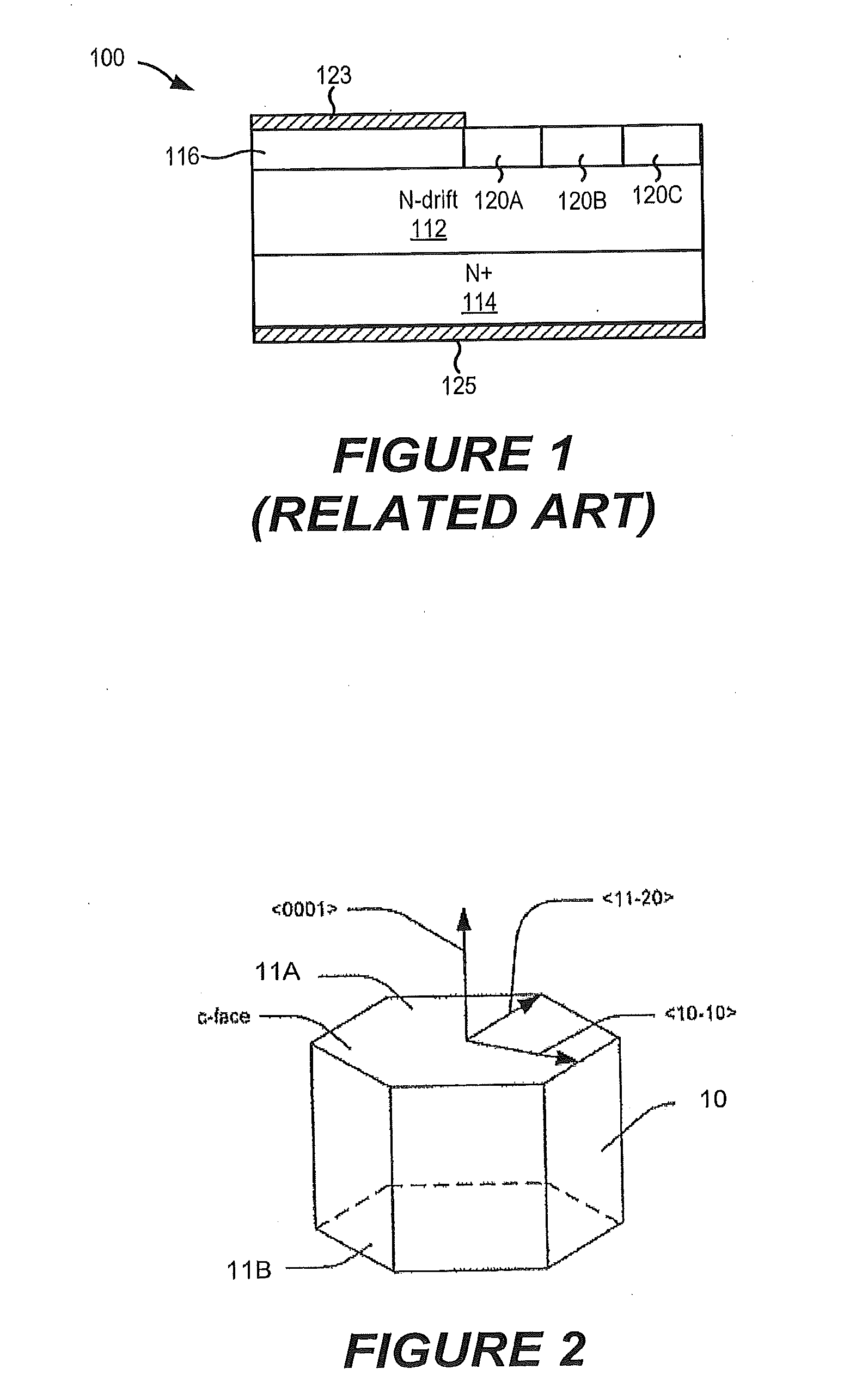
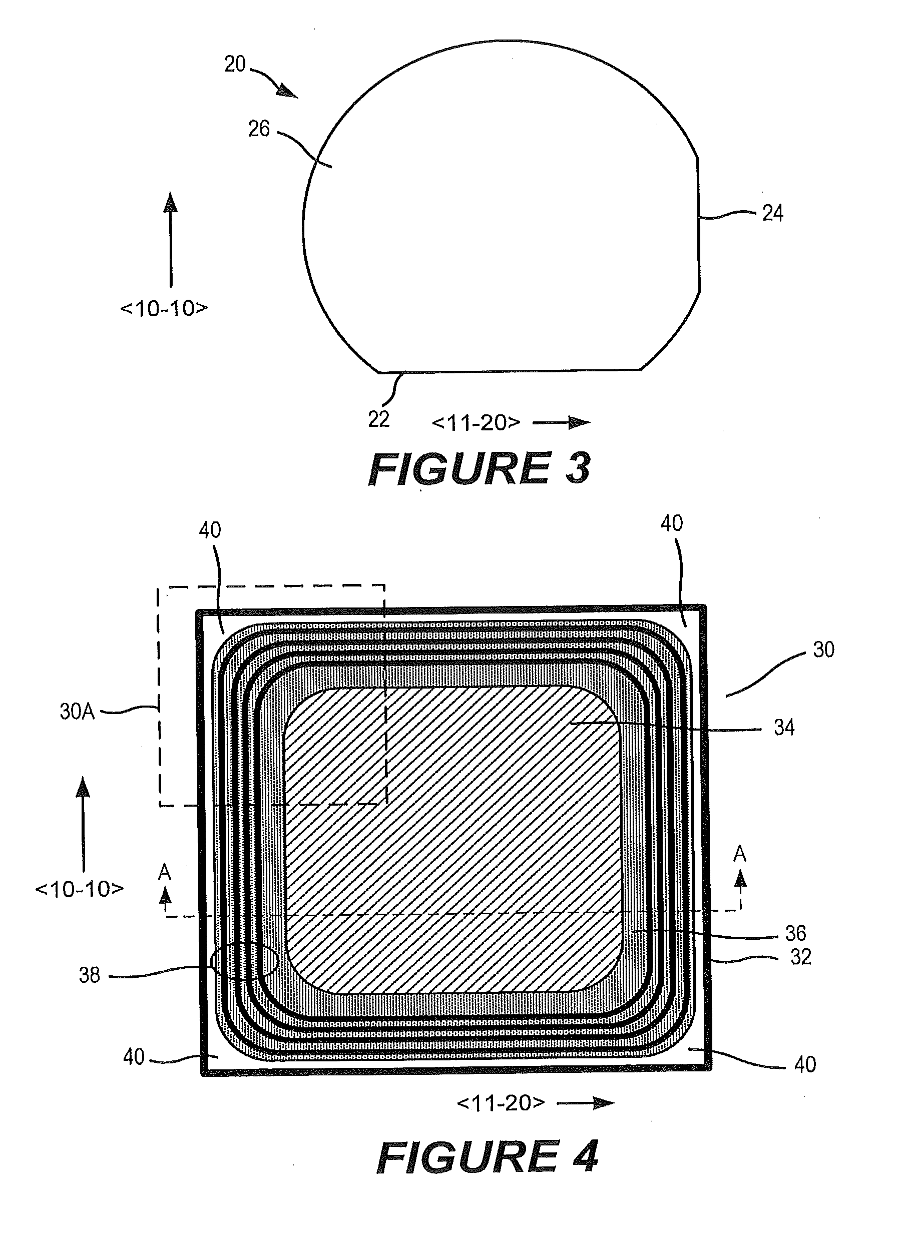
[0042]Embodiments of the present invention now will be described more fully hereinafter with reference to the accompanying drawings, in which embodiments of the invention are shown. This invention may, however, be embodied in many different forms and should not be construed as limited to the embodiments set forth herein. Rather, these embodiments are provided so that this disclosure will be thorough and complete, and will fully convey the scope of the invention to those skilled in the art. Like numbers refer to like elements throughout.

[0043]As is described in more detail below, embodiments of the present invention may provide improved edge termination of semiconductor devices, such as P-N, Schottky, PIN or other such semiconductor devices. Particular embodiments of the present invention provide edge termination for silicon carbide (SiC) devices. For example, embodiments of the present invention may be utilized as edge termination for SiC Schottky diodes, junction barrier Schottky (...


PUM


Abstract

An electronic device includes a semiconductor layer, a primary junction in the semiconductor layer, a lightly doped region surrounding the primary junction and a junction termination structure in the lightly doped region adjacent the primary junction. The junction termination structure has an upper boundary, a side boundary, and a corner between the upper boundary and the side boundary, and the lightly doped region extends in a first direction away from the primary junction and normal to a point on the upper boundary by a first distance that is smaller than a second distance by which the lightly doped region extends in a second direction away from the primary junction and normal to a point on the corner. At least one floating guard ring segment may be provided in the semiconductor layer outside the corner of the junction termination structure. Related methods are also disclosed.

Description

CROSS-REFERENCE TO RELATED APPLICATIONS[0001]This application is a divisional of U.S. patent application Ser. No. 13 / 024,812, filed Feb. 10, 2011 in the United States Patent and Trademark Office, the disclosure of which is incorporated herein by reference in its entirety.FIELD OF THE INVENTION[0002]The present invention relates to microelectronic devices, and more particularly to edge terminations for microelectronic devices.BACKGROUND OF THE INVENTION[0003]High voltage silicon carbide (SiC) devices can be capable of handling high voltages, and may handle as much as about 100 amps or more of current, depending on the size of their active area. High voltage SiC devices have a number of important applications, particularly in the field of power conditioning, distribution and control.[0004]A conventional power device structure has an n-type SiC substrate on which an n-epitaxial layer, which functions as a drift region, is formed. The device typically includes a P-N and / or Schottky junc...

Claims


Application Information

Patent Timeline
IPC IPC(8): H01L29/06
CPCH01L29/0619H01L29/045H01L29/0615H01L29/1608H01L29/8611H01L29/872
Inventor HENNING, JASONZHANG, QINGCHUNRYU, SIE-HYUNG
Owner CREE INC
Why Eureka
Try Eureka