Organic Light Emitting Device and Method of Producing

a light-emitting device and light-emitting diode technology, which is applied in the direction of solid-state devices, semiconductor devices, thermoelectric devices, etc., can solve the problems of light-emitting diodes, light-emitting diodes, and enhancement of the outcoupling efficiency of oleds used in lighting, so as to improve the efficiency of coupling out light and outcoupling efficiency

Active Publication Date: 2014-11-13
NOVALED GMBH
View PDF6 Cites 20 Cited by
  • Summary
  • Abstract
  • Description
  • Claims
  • Application Information

AI Technical Summary

Benefits of technology

[0009]It is an object of the invention to provide an organic light emitting device with improved...

Problems solved by technology

Most of the good performance electron or hole transport materials are relatively high cost materials mainly due to their complex synthetic route, which presents a problem to be solved.
Another problem to be solved is the enhancement of the outcoupling efficiency of OLEDs to be used in lighting.
Typical organic light-emitting diode...

Method used


Image

  • Organic Light Emitting Device and Method of Producing
  • Organic Light Emitting Device and Method of Producing
  • Organic Light Emitting Device and Method of Producing

Examples


Embodiment Construction

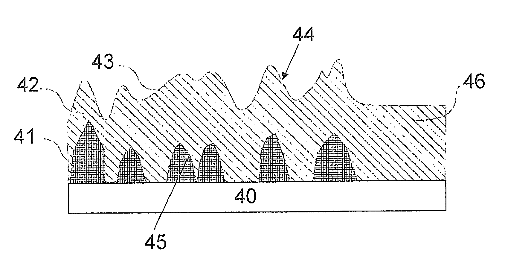
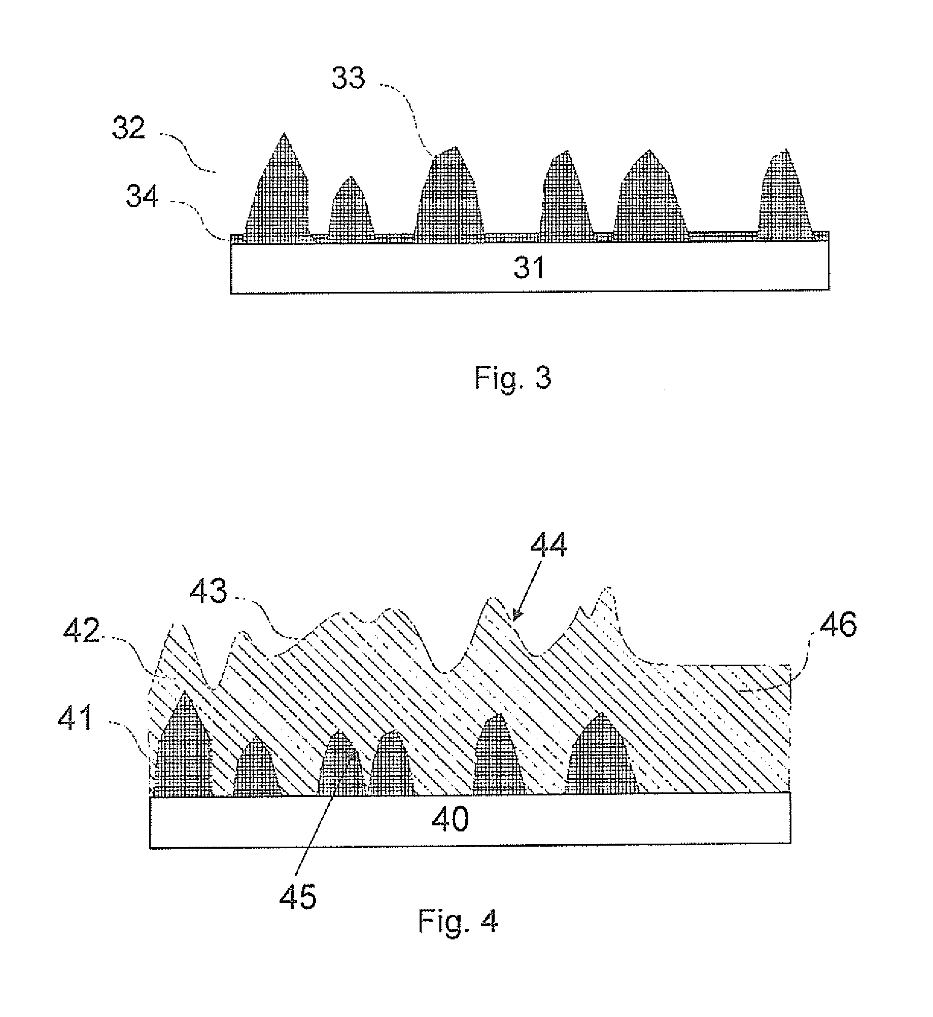
[0012]The roughening layer causes the top electrode to be provided with an electrode roughness by roughening the top electrode on at least one an inner side facing the electrically active region and an outer side of the top electrode facing away from the electrically active region.

[0013]The top electrode roughness may comprise roughened inner surface structures on the inner side of the top electrode which is facing the electrically active region. The top electrode roughness may comprise roughened outer surface structures on the outer side of the top electrode. Looking from above on the electrode, the roughened inner surface structures and the roughened outer surface structures may essentially overlap.

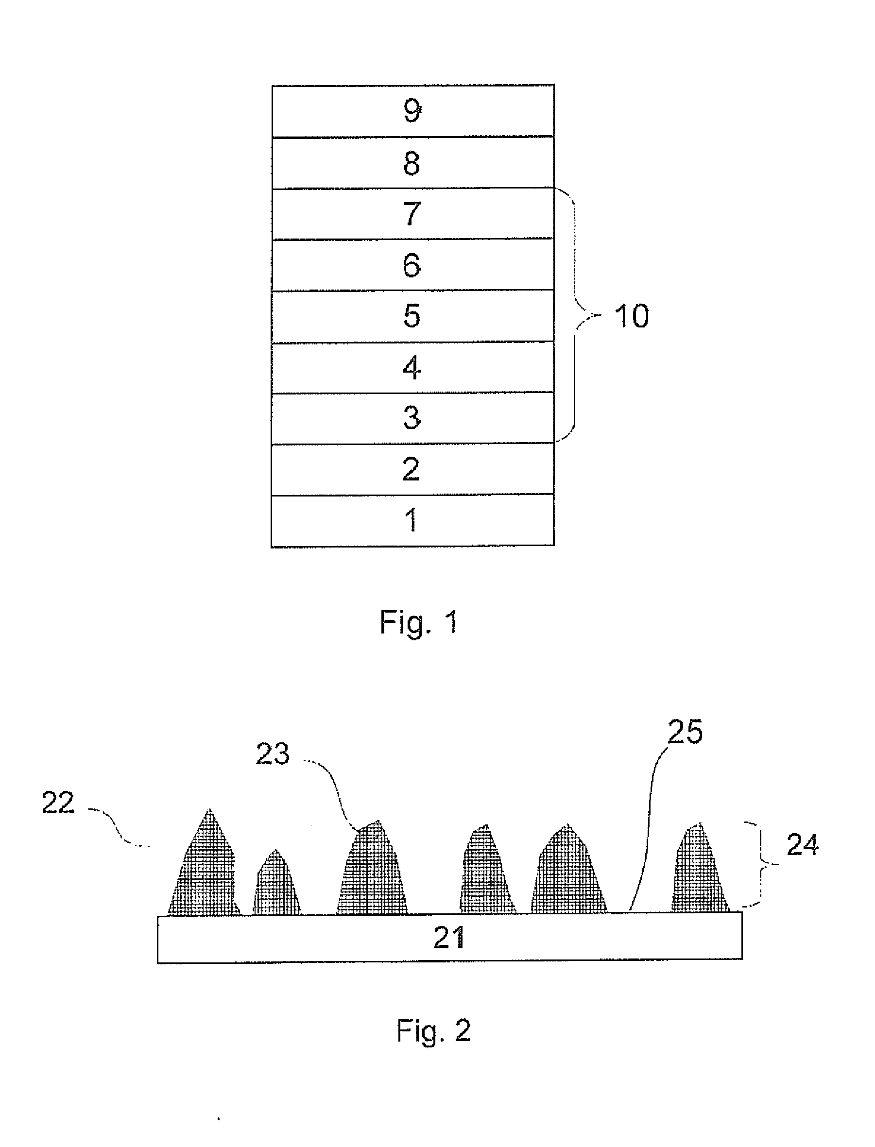
[0014]According to another aspect, an organic light emitting device comprising a layered structure is provided. The layered structure comprises a substrate, a bottom electrode, a top electrode, wherein the bottom electrode is closer to the substrate than the top electrode, and an electr...


PUM


Abstract

The invention relates to an organic light emitting device, in a layered structure, comprising a substrate, a bottom electrode, a top electrode, wherein the bottom electrode is closer to the substrate than the top electrode, an electrically active region, the electrically active region comprising one or more organic layers and being provided between and in electrical contact with the bottom electrode and the top electrode, a light emitting region provided in the electrically active region, and a roughening layer, the roughening layer being provided as non-closed layer in the electrically active region and providing an electrode roughness to the top electrode by roughening the top electrode on at least one an inner side facing the electrically active region and an outer side of the top electrode facing away from the electrically active region. Furthermore, a further organic light emitting device, and a method of producing an organic light emitting device are provided.

Description

FIELD OF THE INVENTION[0001]The present disclosure refers to an organic light emitting device and method of producing.BACKGROUND[0002]Organic semiconductors are used in the production of simple electronic components e.g. resistors, diodes, field effect transistors, and also optoelectronic components like organic light emitting devices, e.g. OLED (organic light emitting diodes), and many others. The industrial and economical significance of the organic semiconductors and their devices is reflected in the increased number of devices using organic semiconducting active layers and the increasing industry focus on the subject.[0003]Organic semiconductor devices are made by layers; such organic semiconducting layers mainly comprise conjugated organic compounds, which can be small molecules, for instance monomers, or oligomers, polymers, copolymers, copolymers of conjugated and non-conjugated blocks, completely or partially cross-linked layers, aggregate structures, or brush like structure...

Claims


Application Information

Patent Timeline
IPC IPC(8): H01L51/00H01L51/52
CPCH01L51/0014H01L51/52H01L2251/56H10K50/822H10K50/854H10K50/805H10K71/20H10K50/80H10K71/00
Inventor BIRNSTOCK, JANMURANO, SVENPAVICIC, DOMAGOJFURNO, MAUROROSENOW, THOMAS
Owner NOVALED GMBH
Why Eureka
Try Eureka