Integrated Multi-Color Light Emitting Device Made With Hybrid Crystal Structure

a technology of hybrid crystal structure and light emitting device, which is applied in the manufacturing of semiconductor/solid-state devices, semiconductor devices, electrical equipment, etc., can solve the problems of difficult integration and fabrication of red and green/blue semiconductor leds as individual red (“r”), green (“g”), blue (“b”) pixels on one wafer

Active Publication Date: 2014-11-20
NASA
View PDF5 Cites 17 Cited by
  • Summary
  • Abstract
  • Description
  • Claims
  • Application Information

AI Technical Summary

Problems solved by technology

Because the atomic crystal structures are different for red LED and green / blue LEDs, the integration and fabrication of these red and green / blue semiconductor LEDs as individual red (“R”), green (“G”), blue (“B”) pixels on one wafer has been extremely difficult.

Method used


Image

  • Integrated Multi-Color Light Emitting Device Made With Hybrid Crystal Structure
  • Integrated Multi-Color Light Emitting Device Made With Hybrid Crystal Structure
  • Integrated Multi-Color Light Emitting Device Made With Hybrid Crystal Structure

Examples


Embodiment Construction

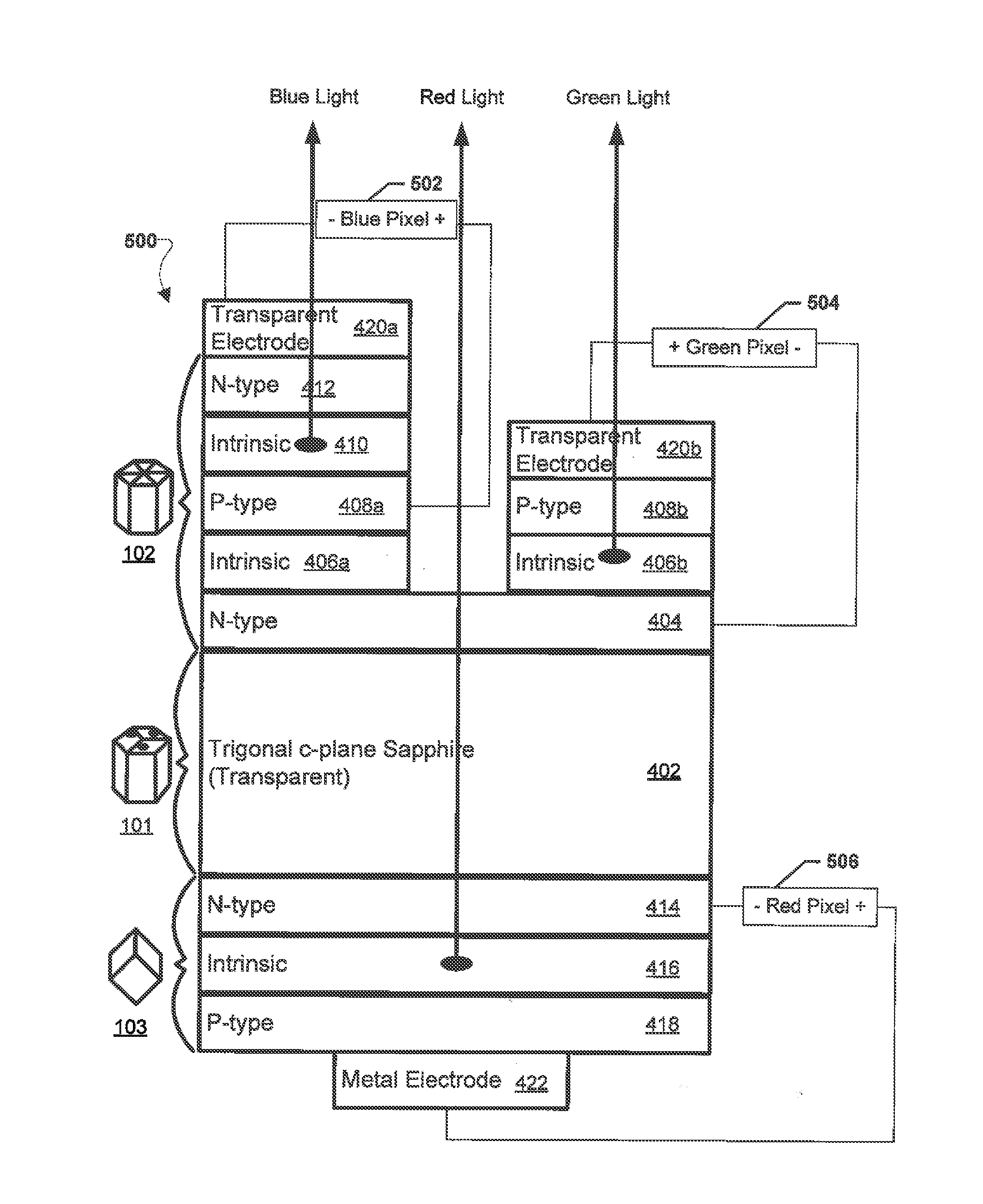
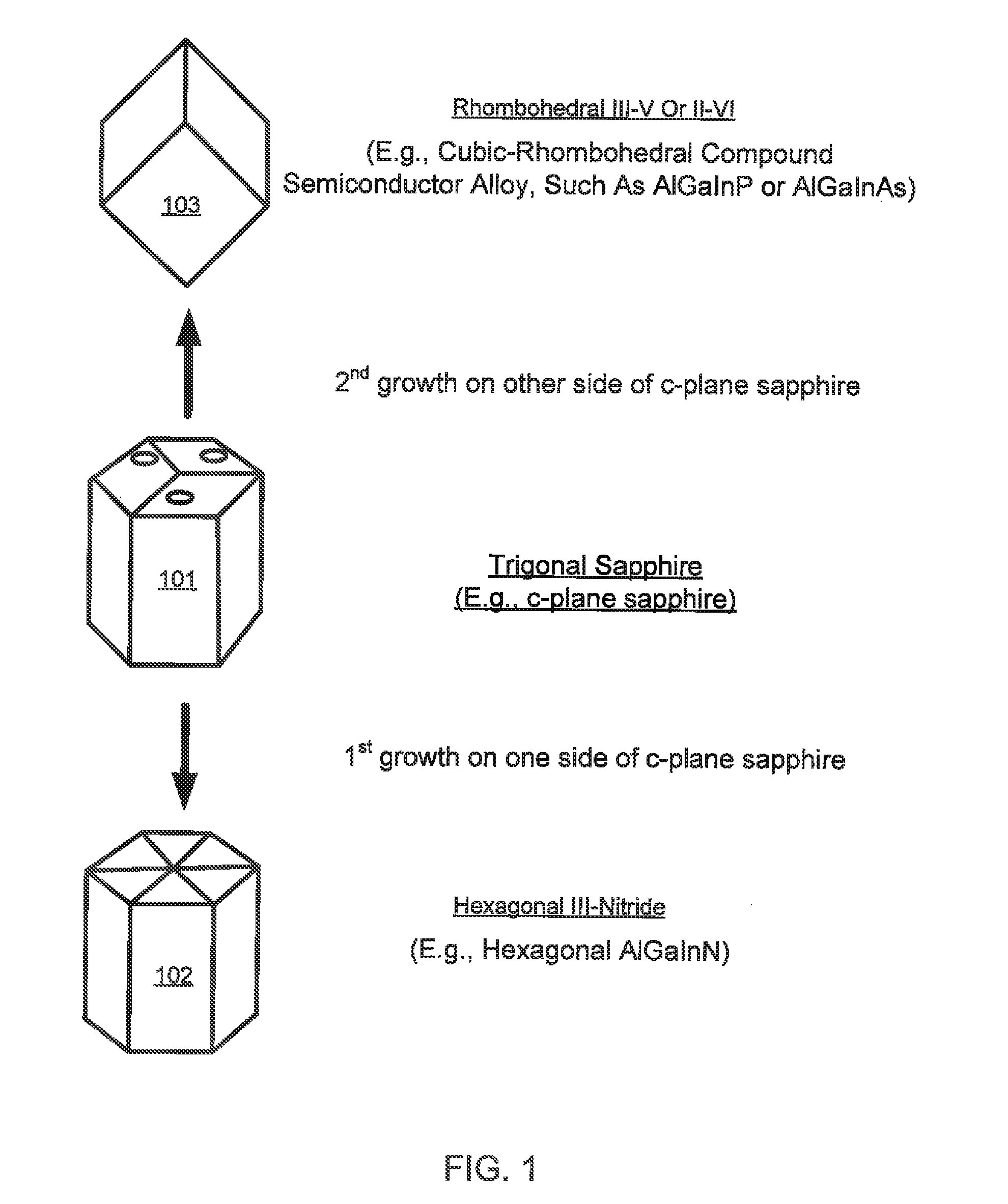
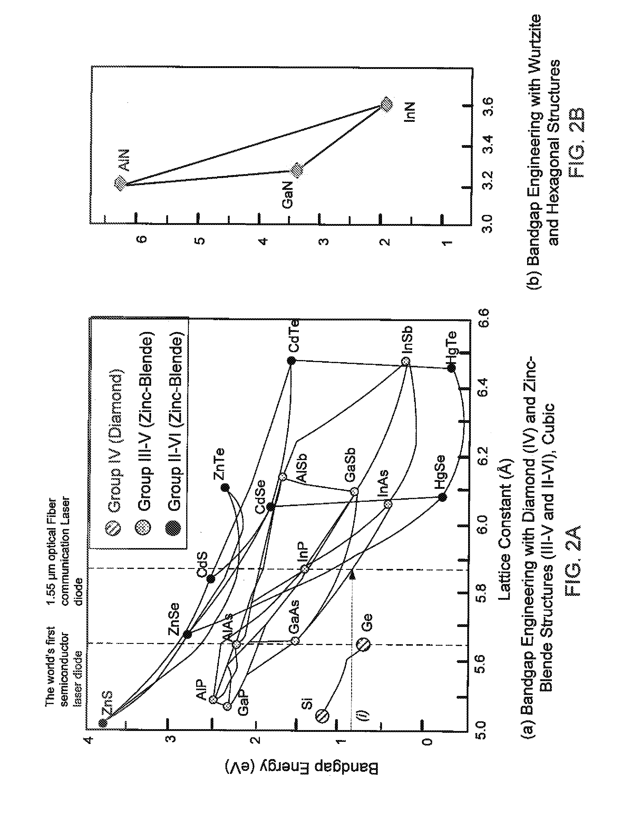
[0017]For purposes of description herein, it is to be understood that the specific devices and processes illustrated in the attached drawings, and described in the following specification, are simply exemplary embodiments of the inventive concepts defined in the appended claims. Hence, specific dimensions and other physical characteristics relating to the embodiments disclosed herein are not to be considered as limiting, unless the claims expressly state otherwise.

[0018]The word “exemplary” is used herein to mean “serving as an example, instance, or illustration.” Any implementation described herein as “exemplary” is not necessarily to be construed as preferred or advantageous over other implementations.

[0019]The various embodiments will be described in detail with reference to the accompanying drawings. Wherever possible, the same reference numbers will be used throughout the drawings to refer to the same or like parts. References made to particular examples and implementations are...


PUM


Abstract

An integrated hybrid crystal Light Emitting Diode (“LED”) display device that may emit red, green, and blue colors on a single wafer. The various embodiments may provide double-sided hetero crystal growth with hexagonal wurtzite III-Nitride compound semiconductor on one side of (0001) c-plane sapphire media and cubic zinc-blended III-V or II-VI compound semiconductor on the opposite side of c-plane sapphire media. The c-plane sapphire media may be a bulk single crystalline c-plane sapphire wafer, a thin free standing c-plane sapphire layer, or crack-and-bonded c-plane sapphire layer on any substrate. The bandgap energies and lattice constants of the compound semiconductor alloys may be changed by mixing different amounts of ingredients of the same group into the compound semiconductor. The bandgap energy and lattice constant may be engineered by changing the alloy composition within the cubic group IV, group III-V, and group II-VI semiconductors and within the hexagonal III-Nitrides.

Description

CROSS REFERENCE TO RELATED APPLICATIONS[0001]This application claims the benefit of priority to U.S. Provisional Application No. 61 / 824,017 filed on May 16, 2013 entitled “INTEGRATED MULTI-COLOR LIGHT EMITTING DEVICE MADE WITH HYBRID CRYSTAL STRUCTURE”, the entire contents of which are hereby incorporated by reference in their entirety.STATEMENT REGARDING FEDERALLY SPONSORED RESEARCH OR DEVELOPMENT[0002]The invention described herein was made in the performance of work under a NASA contract and by an employee of the United States Government and is subject to the provisions of Public Law 96-517 (35 U.S.C. §202) and may be manufactured and used by or for the Government for governmental purposes without the payment of any royalties thereon or therefore. In accordance with 35 U.S.C. §202, the contractor elected not to retain title.BACKGROUND OF THE INVENTION[0003]1. Field of the Invention[0004]The present invention relates to a hybrid crystal light emitting diode (“LED”) display device ...

Claims


Application Information

Patent Timeline
Patent Type & Authority Applications(United States)
IPC IPC(8): H01L33/08H01L33/00
CPCH01L33/08H01L33/002H01L33/005H01L27/15H01L33/007H01L33/16H01L33/0066H01L33/0075H01L33/0087
Inventor PARK, YEONJOONCHOI, SANG HYOUK
Owner NASA
Why Eureka
Try Eureka