Semiconductor system

Active Publication Date: 2014-11-20
SK HYNIX INC
View PDF12 Cites 4 Cited by
  • Summary
  • Abstract
  • Description
  • Claims
  • Application Information

AI Technical Summary

Benefits of technology

The present invention relates to a semiconductor system capable of detecting errors in data transmission. The system includes a semiconductor circuit and a controller. The semiconductor circuit generates an error detection code based on the data provided from a data input / output unit and compares it with an expected code generated from the controller. The controller generates an error detection code based on the data provided from the same data input / output unit. The second error detection code is compared with the first error detection code to detect any errors in the data transmission. The system can also output an error address signal when an error is detected. The technical effect of this invention is to provide a reliable and efficient means for detecting errors in data transmission and ensuring the accuracy of data transmission.

Problems solved by technology

Due to various causes including noise introduced into a transmission line, an error may occur in data transmitted between a first device (for example, a semiconductor circuit) and a second device (for example, a controller to control the semiconductor circuit or a tester for testing the semiconductor circuit).

Method used


Image

  • Semiconductor system
  • Semiconductor system
  • Semiconductor system

Examples


Embodiment Construction

[0019]Hereinafter, a semiconductor system according to the present invention will be described below with reference to the accompanying drawings through various examples of embodiments.

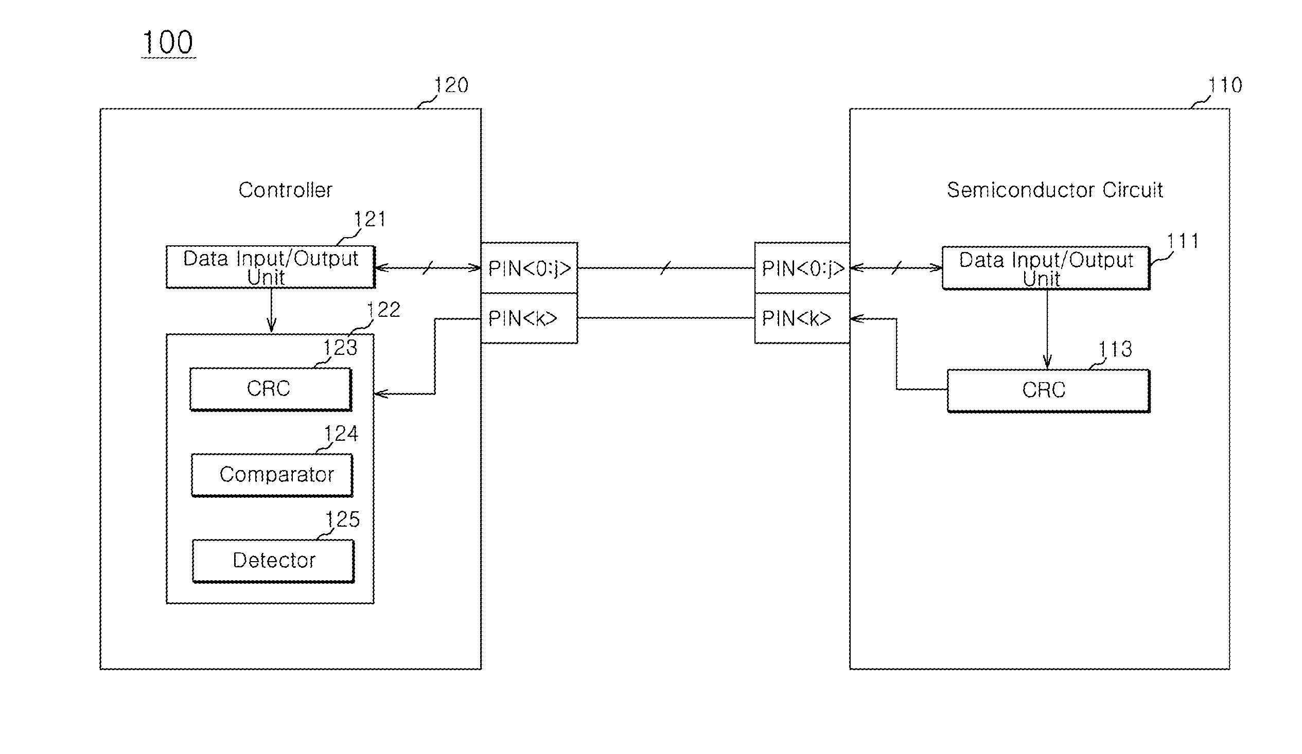
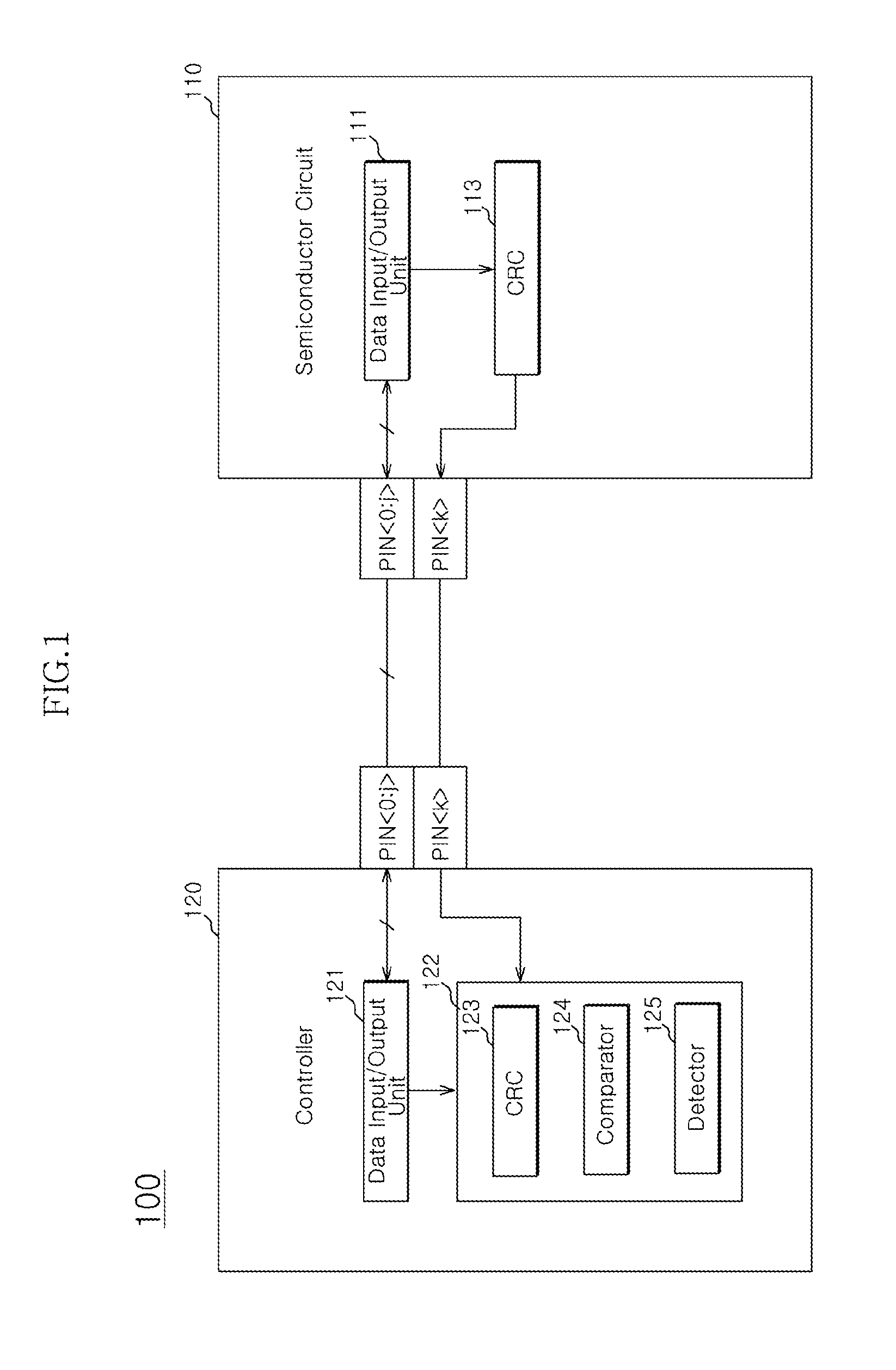
[0020]FIG. 1 is a block diagram illustrating the configuration of a semiconductor system 100 according to an embodiment of the present invention.

[0021]FIG. 1 illustrates an example of a semiconductor system based on a semiconductor circuit and a controller.

[0022]Referring to FIG. 1, the semiconductor system 100 according to the embodiments of the present invention may include a semiconductor circuit 110 and a controller 120.

[0023]The semiconductor circuit 110 may include input / output pins PIN coupled to input / output pins PIN of the controller 120, respectively.

[0024]Additionally, error information may be transmitted through any one of the input / output pins PIN, for example, the input / output pin PIN, and data may be transmitted through the other input / output pins PIN.

[0025]The semiconductor circuit 110...


PUM


Abstract

A semiconductor system including a semiconductor circuit configured to compare a first error detection code generated by performing an operation on read data to a second error detection code and determine a data transmission error, and a controller configured to provide the second error detection code, generated by performing an operation on expect data based on the read data, to the semiconductor circuit.

Description

CROSS-REFERENCES TO RELATED APPLICATION[0001]The present application claims priority under 35 U.S.C. §119(a) to Korean application number 10-2013-0056427, filed on May 20, 2013, in the Korean Intellectual Property Office, which is incorporated herein by reference in its entirety.BACKGROUND[0002]1. Technical Field[0003]Various embodiments relate to a semiconductor circuit, and more particularly, to a semiconductor system.[0004]2. Related Art[0005]Due to various causes including noise introduced into a transmission line, an error may occur in data transmitted between a first device (for example, a semiconductor circuit) and a second device (for example, a controller to control the semiconductor circuit or a tester for testing the semiconductor circuit).[0006]Thus, there is a demand for a method for checking and detecting whether or not the data was or is being normally transmitted between the two devices.SUMMARY[0007]Various embodiments are directed to a semiconductor system capable o...

Claims


Application Information

Patent Timeline
IPC IPC(8): G06F11/10
CPCG06F11/10G06F11/1004G11C7/10G11C29/42
Inventor LEE, HYENG OUK
Owner SK HYNIX INC
Why Eureka
Try Eureka