Supercharge Your Innovation With Domain-Expert AI Agents!

Substrate processing apparatus

a substrate and processing technology, applied in the direction of cleaning processes and apparatus, chemistry apparatus and processes, cleaning using liquids, etc., can solve the problem and achieve the effect of increasing the manufacturing cost of the substrate processing apparatus

Active Publication Date: 2014-12-04
DAINIPPON SCREEN MTG CO LTD
View PDF2 Cites 3 Cited by
  • Summary
  • Abstract
  • Description
  • Claims
  • Application Information

AI Technical Summary

Benefits of technology

The present invention aims to prevent electrical arcing on a substrate during the process of applying processing liquid. The invention provides a way to reduce this risk without increasing the cost of the substrate processing apparatus.

Problems solved by technology

Though it is thought to form the whole cup part with antistatic plastic material as disclosed in Document 1, such special material is expensive to greatly increase the manufacturing cost of the substrate processing apparatus.

Method used


Image

  • Substrate processing apparatus
  • Substrate processing apparatus
  • Substrate processing apparatus

Examples


Embodiment Construction

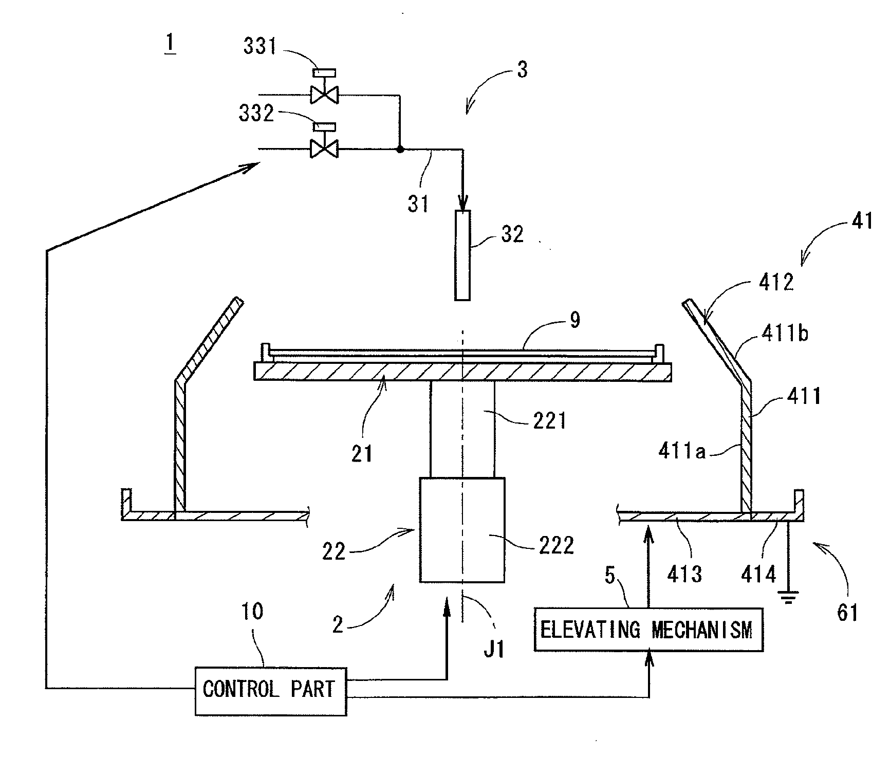
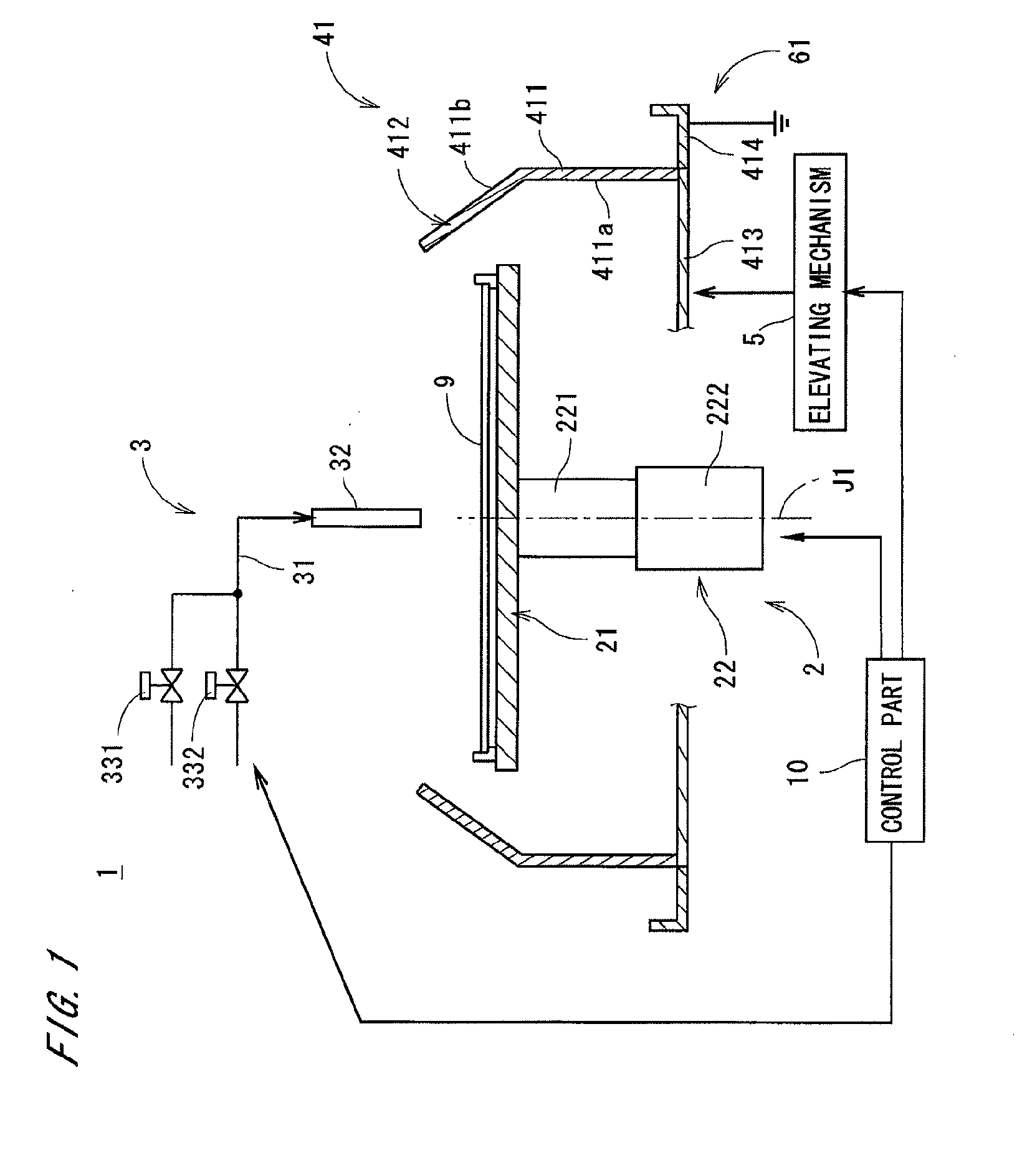
[0042]FIG. 1 is a view showing a construction of a substrate processing apparatus 1 in accordance with the first preferred embodiment of the present invention. The substrate processing apparatus 1 is an apparatus for performing processings such as etching which is performed by applying processing liquid onto a semiconductor substrate 9 (for example, a silicon substrate, and hereinafter simply referred to as “substrate 9”) on which an insulating film (e.g., an oxide film) is formed.

[0043]As shown in FIG. 1, the substrate processing apparatus 1 has a substrate holding part 2 for holding the substrate 9 in contact with a lower main surface of the substrate 9, a processing liquid applying part 3 which is positioned above the substrate 9 to eject cleaning liquid onto an upper main surface of the substrate 9 (hereinafter, referred to as “upper surface”), a cup part 41 surrounding the substrate holding part 2, an elevating mechanism 5 which is a cylinder mechanism for moving the cup part 4...


PUM


Abstract

A substrate processing apparatus has a cup part for receiving processing liquid such as pure water which is splashed from a substrate. The cup part is formed of electrical insulation material or semiconductor material. Hydrophilic treatment may be performed on an outer annular surface of the cup part and water may be held on the outer annular surface of the cup part while processing the substrate. With the disclosed apparatus, charged potential of the cup part generated by splashing of pure water can be suppressed, without greatly increasing the manufacturing cost of the substrate processing apparatus. As a result, it is possible to prevent electric discharge from occurring on the substrate due to induction charging of the substrate, in application of the processing liquid onto the substrate.

Description

BACKGROUND OF THE INVENTION[0001]1. Field of the Invention[0002]The present invention relates to a technique for processing a substrate by applying processing liquid onto the substrate.[0003]2. Description of the Background Art[0004]In a manufacturing process of a semiconductor substrate (hereinafter, simply referred to as “substrate”), various processings have been conventionally performed on the substrate, on which an insulating film such as an oxide film is formed, with using a substrate processing apparatus. For example, a processing of etching or the like is performed on a surface of the substrate by applying processing liquid onto the substrate while rotating the substrate around the central axis perpendicular to its main surface. Processing liquid splashed from the rotating substrate is received by a cup part (splash guard) surrounding the substrate, thereby preventing the processing liquid from being splashed outside the apparatus. Such a cup part is normally formed of elect...

Claims


Application Information

Patent Timeline
Patent Type & Authority Applications(United States)
IPC IPC(8): H01L21/67
CPCH01L21/67051H01L21/304B08B3/04H01L21/461
Inventor MIYAGI, MASAHIROSATO, MASANOBUARAKI, HIROYUKI
Owner DAINIPPON SCREEN MTG CO LTD
Features
  • R&D
  • Intellectual Property
  • Life Sciences
  • Materials
  • Tech Scout
  • Unparalleled Data Quality
  • Higher Quality Content
  • 60% Fewer Hallucinations
Learn More