Plasma etching equipment

a technology of etching equipment and plasma, which is applied in the direction of electrical equipment, basic electric elements, electric discharge tubes, etc., can solve the problems of affecting the quality of etching equipment, material erosion damage, and material contamination, and achieve the effect of reducing particles or contamination in samples

Inactive Publication Date: 2008-10-02
HITACHI HIGH-TECH CORP
View PDF7 Cites 40 Cited by
  • Summary
  • Abstract
  • Description
  • Claims
  • Application Information

AI Technical Summary

Benefits of technology

[0011]It is an object of the present invention to provide a plasma processing equipment that can reduce parti...

Problems solved by technology

Generally, in the manufacturing process of a semiconductor device, a liquid crystal device, and the like, a process gas including a fluoride such as BF3 or NF3, a chloride such as BCl3 or SnCl4, or a bromide such as HBr is used inside the processing chamber, and therefore there is a problem that an inner wall material of an etching processing chamber is corroded and worn significantly.
Moreover, it is also known that these materials are subjected to erosion damage due to ions excited by the plasma.
However, under such environment using plasma, the halogenated compound is dissociated to produce extremely highly corrosive atomic F, Cl, Br, and the like, and also if a fine powder-form solid of SiO2, Si3N4, Si, W, or the like is present in this environment, a member used inside the plasma processing chamber is subjected to chemical corrosion as well as to erosion damage due to the microparticles, resulting in being subjected to the so-called erosion-corrosion effect, strongly.
In addition, it is also known that in an environment in which plasma processing chamb...

Method used


Image

  • Plasma etching equipment
  • Plasma etching equipment
  • Plasma etching equipment

Examples


examples

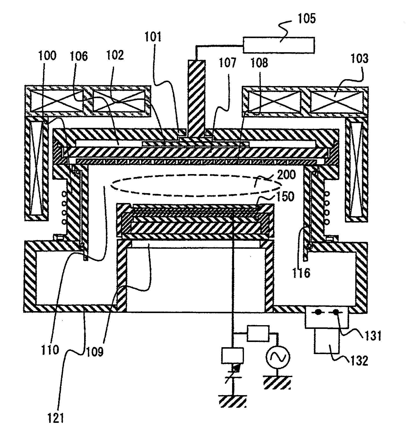
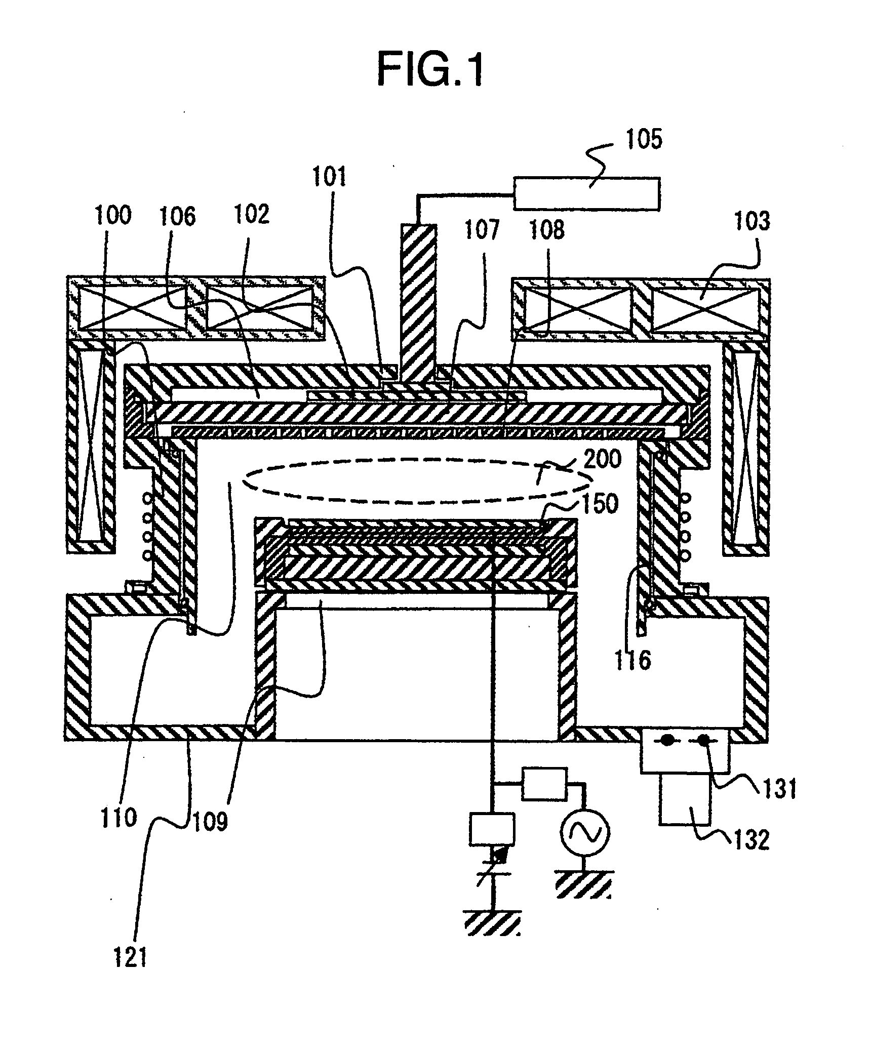
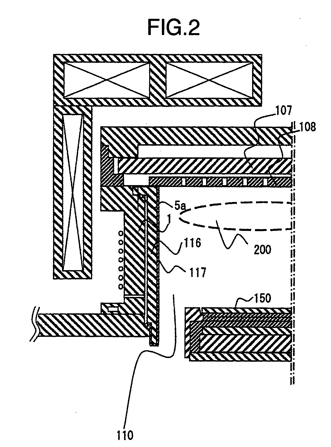
[0052]Hereinafter, an example of the present invention will be described using FIG. 1, FIG. 2, and a FIG. 3 and FIG. 4. FIG. 1 is a vertical cross-sectional view showing a configuration of a chamber part of a processing unit.

[0053]As shown in this view, a processing chamber is disposed in the upper part of processing chambers 100, and this processing chamber comprises: a lid member 101 constituting a lid of a vacuum vessel; an antenna 102 disposed inside this lid member 101; a magnetic field generator 103 disposed on the side of and above this antenna 102 and disposed surrounding the processing chamber; and a ceiling member disposed under this antenna 102. Moreover, above the magnetic field generator 103 there is disposed a radio source part 105 for supplying an electric power for VHF and UHF band frequency from 200 MHz to 1 GHz, which the antenna 102 radiates. The antenna 102 to supply is disposed inside the lid member 101 composed of an electrically conductive member, such as SUS,...


PUM

PropertyMeasurementUnit
Electrical resistivityaaaaaaaaaa
Electrical conductoraaaaaaaaaa

Abstract

To provide a plasma processing equipment that can reduce the particles or contamination in a sample by suppressing the occurrence of an abnormal electric discharge during processing. The plasma processing equipment that employs a plasma process using a halogen-based gas in fabricating a semiconductor device, wherein a plasma sprayed coating film is applied to a surface of a well, such as a wall in a processing chamber, which plasma is in constant with, and wherein a conductor is incorporated into a material of this plasma sprayed coating film, thereby making the plasma sprayed coating film conductive.

Description

INCORPORATION BY REFERENCE[0001]The present application claims priority from Japanese application JP2007-090141 filed on Mar. 30, 2007, the content of which is hereby incorporated by reference into this application.FIELD OF THE INVENTION[0002]The present invention relates to a plasma processing equipment that processes a substrate-shaped sample, such as a semiconductor wafer, arranged inside a processing chamber in a vacuum vessel using plasma formed in this processing chamber. In particular, the present invention relates to the plasma processing equipment that includes inside the processing chamber a member having a potential of a predetermined value with respect to the plasma.BACKGROUND OF THE INVENTION[0003]As the conventional plasma etching equipment, as described in JP patent Appln. No. 11-351546 (JP-A-2001-164354) (Patent Document 1), it is known that the coating of the surface of a processing chamber container with a plasma sprayed coating of Y2O3 or the like having a porosit...

Claims


Application Information

Patent Timeline
IPC IPC(8): H01L21/306
CPCH01J37/32477H01J37/32623H01L21/3065
Inventor FURUSE, MUNEOKIMURA, SHINGOKAWAGUCHI, TADAYOSHI
Owner HITACHI HIGH-TECH CORP
Why Eureka
Try Eureka