Imaging Array with Improved Dynamic Range Utilizing Parasitic Photodiodes

Active Publication Date: 2015-01-08
BAE SYST IMAGING SOLUTIONS
View PDF6 Cites 15 Cited by
  • Summary
  • Abstract
  • Description
  • Claims
  • Application Information

AI Technical Summary

Benefits of technology

[0009]In another aspect of the invention, the floating diffusion node includes an n-type implanted region in a p-type semiconductor substrate. The main photodiode also includes an n-type implanted region in the p-type s

Problems solved by technology

In principle, the maximum well capacity can be increased by utilizing larger photodiodes; however, this solution increases the cost of the imaging array and requires processing electronics that can deal with the larger

Method used


Image

  • Imaging Array with Improved Dynamic Range Utilizing Parasitic Photodiodes
  • Imaging Array with Improved Dynamic Range Utilizing Parasitic Photodiodes
  • Imaging Array with Improved Dynamic Range Utilizing Parasitic Photodiodes

Examples


Example

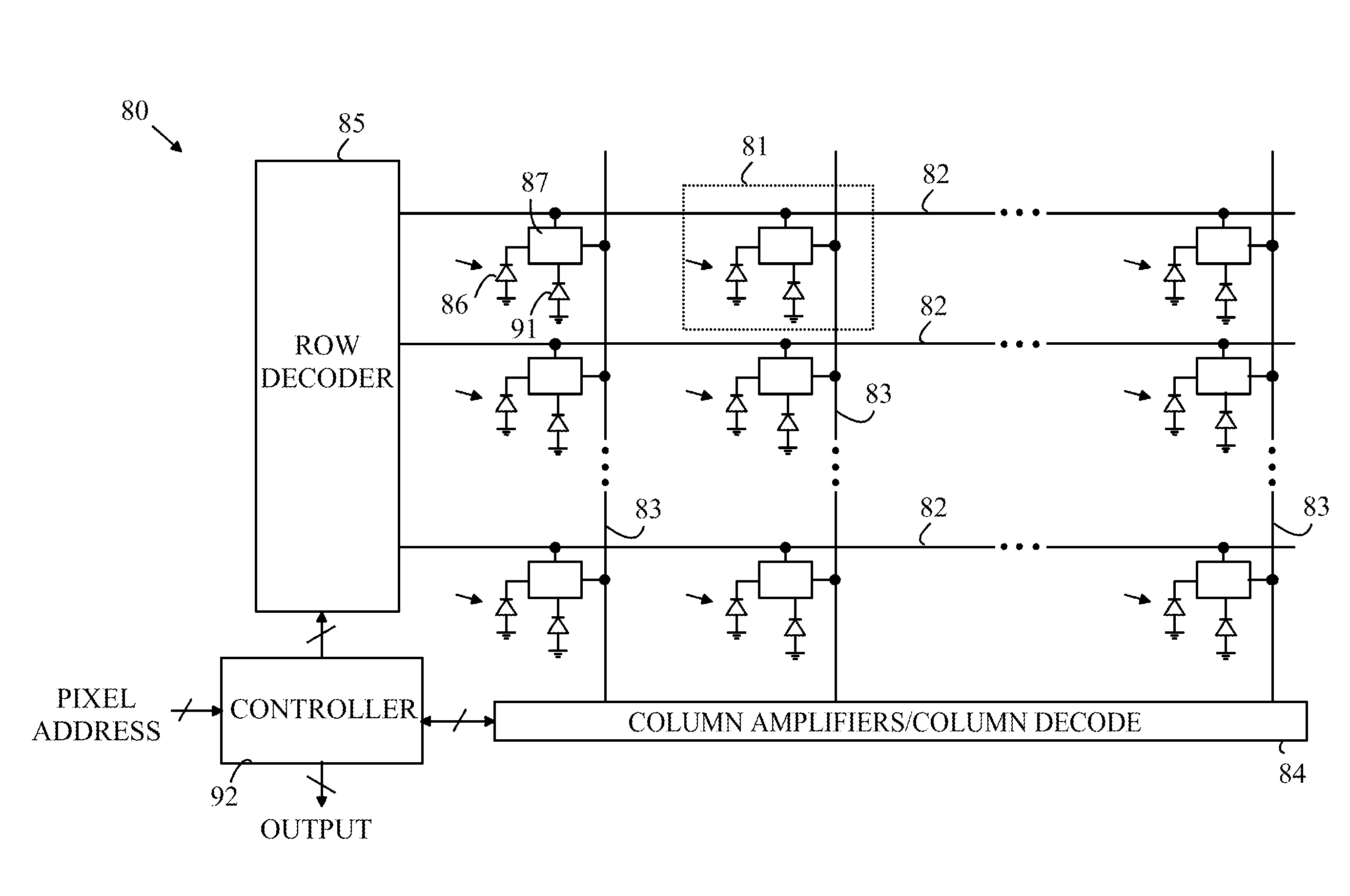
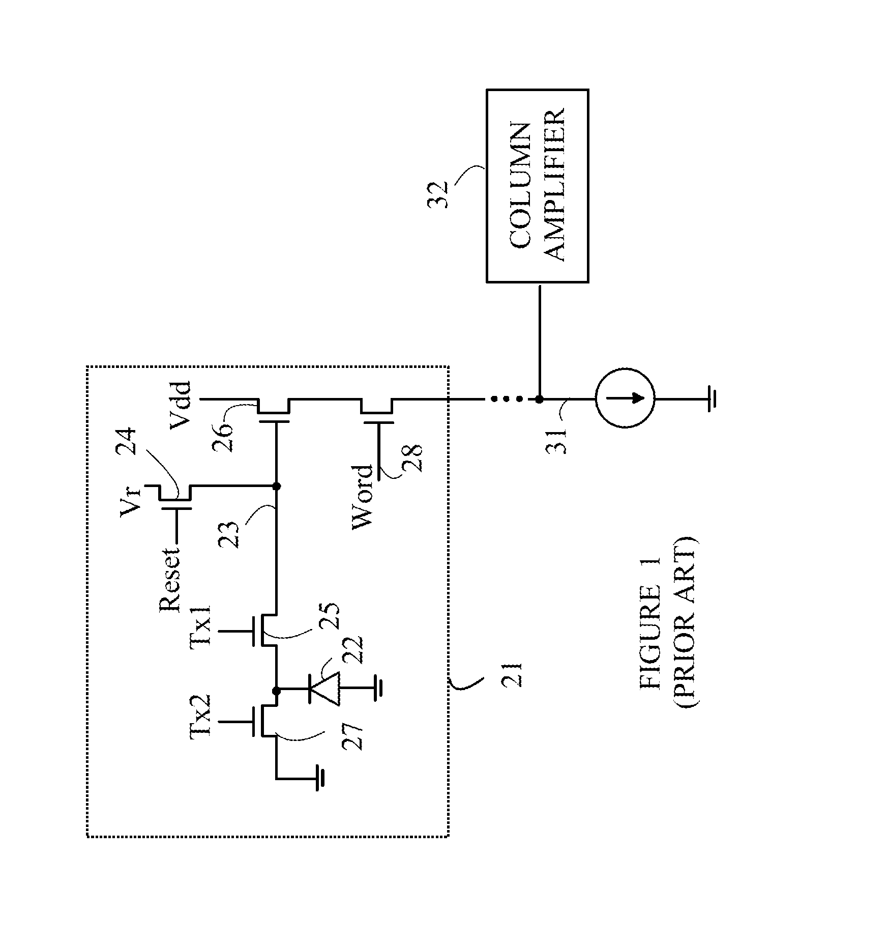
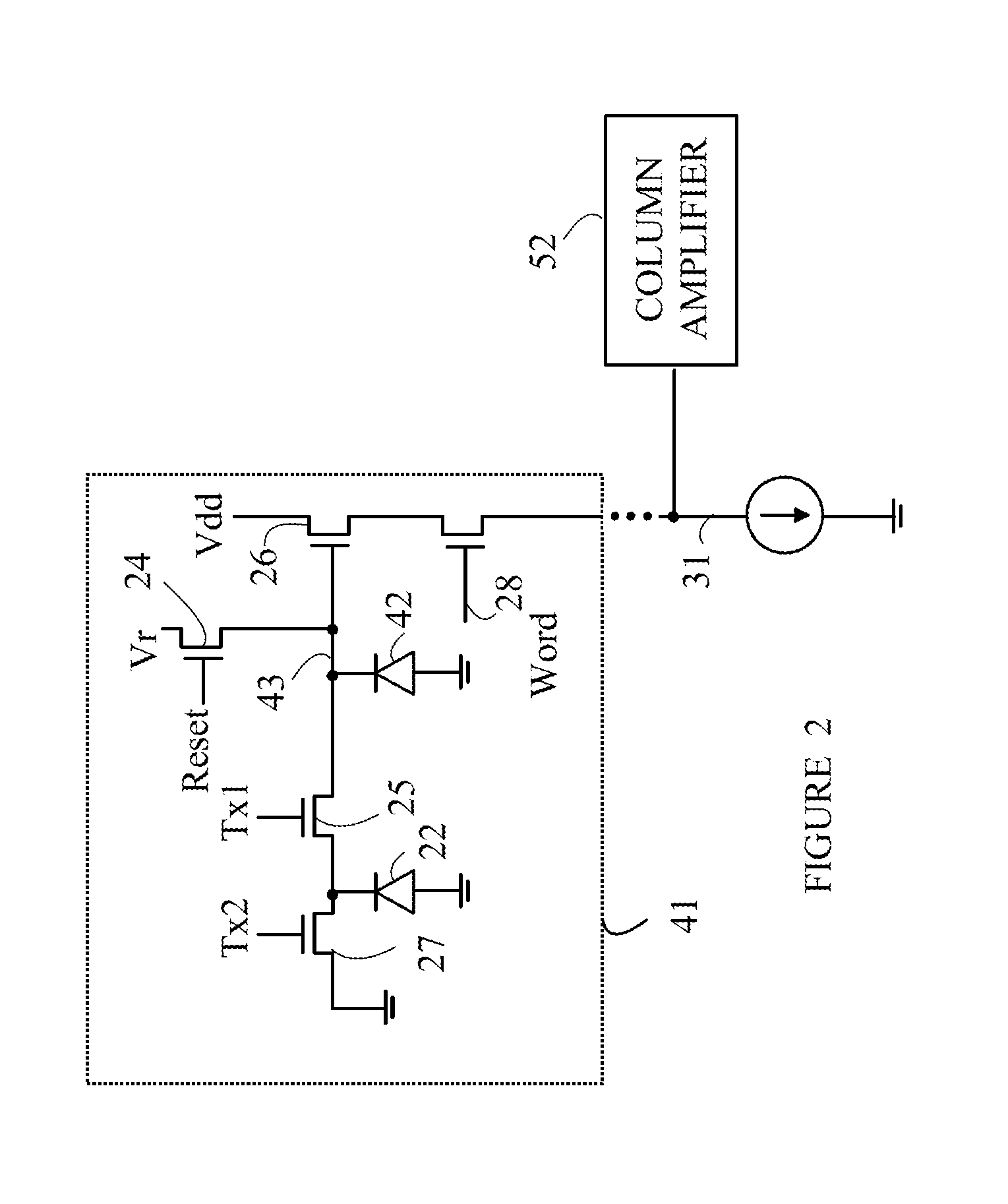
[0016]The manner in which the present invention provides its advantages can be more easily understood with reference to FIG. 1, which is a schematic drawing of a typical prior art pixel sensor in one column of pixel sensors in an imaging array. Pixel sensor 21 includes a photodiode 22 that measures the light intensity at a corresponding pixel in the image. Initially, photodiode 22 is reset by placing gate 25 in a conducting state and connecting floating diffusion node 23 to a reset voltage, Vr. Gate 25 is then closed and photodiode 22 is allowed to accumulate photoelectrons. A potential on gate 27 sets the maximum amount of charge that can be accumulated on photodiode 22. If more charge is accumulated than allowed by the potential on gate 27, the excess charge is shunted to ground through gate 27.

[0017]After photodiode 22 has been exposed, the charge accumulated in photodiode 22 is then measured using a correlated double sampling algorithm. In this algorithm, floating diffusion node...


PUM


Abstract

A pixel sensor having a main photodetector and a parasitic photodiode and a method for reading out that pixel sensor are disclosed. The pixel sensor is read by reading a first potential on a floating diffusion node in the pixel sensor while the floating diffusion node is isolated from the main photodiode. The pixel sensor is then exposed to light such that the floating diffusion node and the photodetector are both exposed to the light. A second potential on the floating diffusion node is then readout while the floating diffusion node is isolated from the main photodiode. After the first and second potentials are readout, a third potential on the floating diffusion node is readout. The main photodiode is then connected to the floating diffusion node, and a fourth potential on the floating diffusion node is readout. First and second light intensities are determined from the readout potentials.

Description

BACKGROUND OF THE INVENTION[0001]CMOS imaging sensors are widely used in cameras and other imaging applications. The imaging sensors typically include a two-dimensional array of pixel sensors. Each pixel sensor includes a photodiode that measures the image intensity at a corresponding point in the image. The dynamic range of the image sensor is the ratio of the minimum amount of light that can be measured to the maximum amount. An image is formed by first emptying the photodiodes of any accumulated charge and then exposing the photodiodes to the image. Each photodiode accumulates charge at a rate determined by the light intensity emitted by the image at the corresponding point in the image, referred to as a pixel. In general, the amount of charge that can be accumulated in a photodiode has a maximum value, referred to as the maximum well capacity. Once this capacity is reached, the excess charge is removed from the pixel through a special gate that shunts the excess charge to ground...

Claims


Application Information

Patent Timeline
IPC IPC(8): H01L27/146
CPCH01L27/14643H01L27/14609H01L27/14656H01L27/14654H01L27/1461H04N25/585H04N25/77H04N23/54H04N25/75
Inventor FOWLER, BOYD
Owner BAE SYST IMAGING SOLUTIONS
Why Eureka
Try Eureka