Emission signal visualization device

a technology of emission signal and visualization device, which is applied in the direction of optical radiation measurement, instruments, spectrometry/spectrophotometry/monochromators, etc., can solve the problems of industrial devices influencing adversely other electronic devices, and achieve the effect of improving the accuracy of measurement results

Active Publication Date: 2015-01-29
NOISE LAB
View PDF0 Cites 20 Cited by
  • Summary
  • Abstract
  • Description
  • Claims
  • Application Information

AI Technical Summary

Benefits of technology

[0012]The present invention has been achieved in order to solve the above problem, and an object of the present invention is to obtain an emission signal visualization device capable of knowing in detail distribution, intensity, etc. of noises in a three-dimensional space around a measured object.

Problems solved by technology

It has been known that unnecessary electromagnetic field noises (hereinafter, simply referred to as noises) generated from electronic, information, communication, and industrial devices influence adversely, such as malfunction, on other electronic devices.

Method used


Image

  • Emission signal visualization device
  • Emission signal visualization device
  • Emission signal visualization device

Examples


modified embodiment

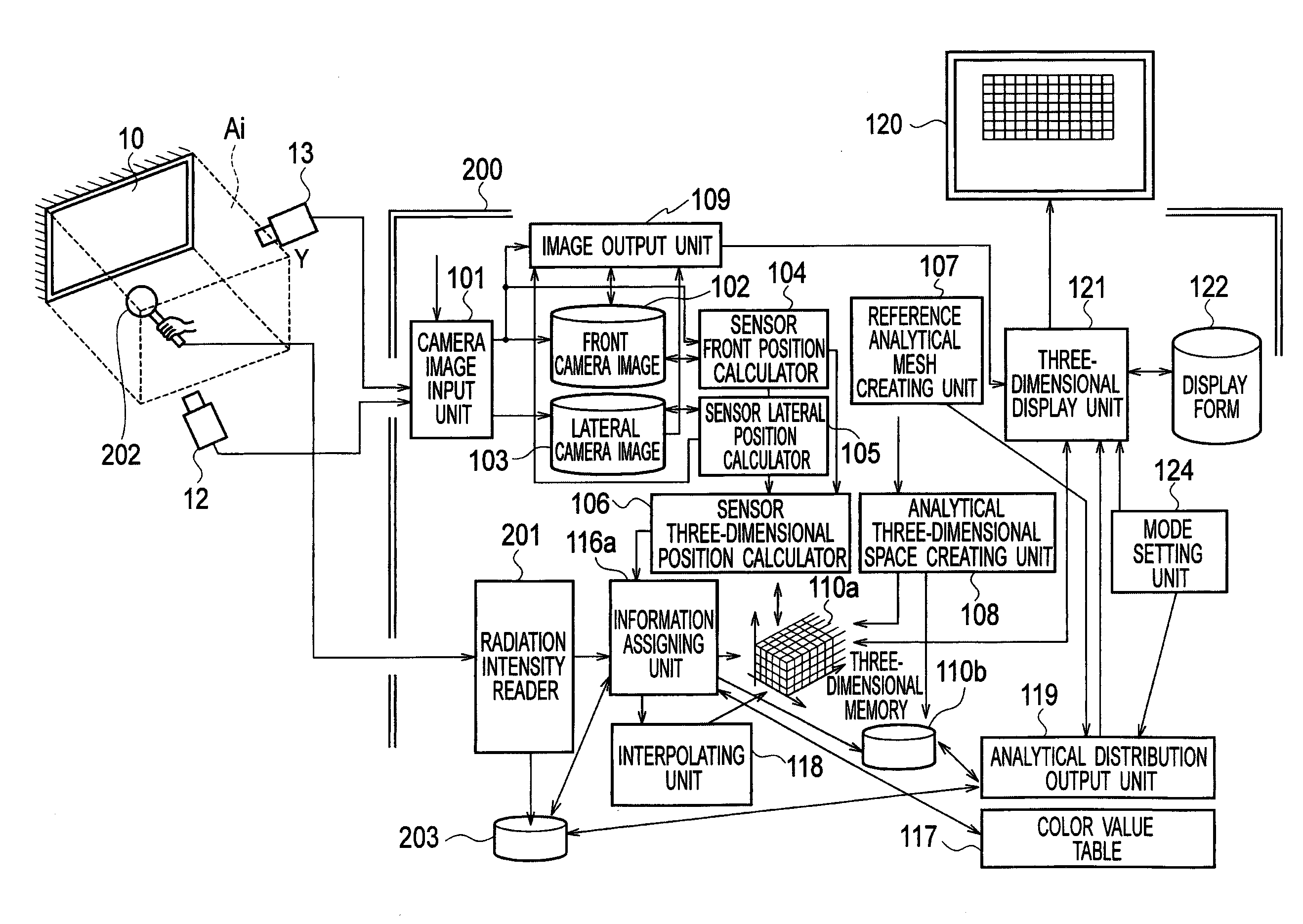
[0288]FIG. 24 is an outline configuration diagram of the emission signal visualization device of another embodiment. In FIG. 24, description is omitted for the same configuration as FIG. 5.

[0289]A measured object should not be limited to an IC substrate, a television set, etc., and may be electronic devices, buildings, foods, etc. which bear radiation. In this case, an emission signal visualization device is configured to display in a color the distribution of radiation from a measured object, and to visualize it.

[0290]In this embodiment, a radiation detecting sensor 202 is used as a sensor.

[0291]Further, a body unit 200 includes a radiation intensity reader 201. Further, it includes an information assigning unit 116a. The information assigning unit 116a is the same as the electromagnetic field information assigning unit 116.

[0292]The radiation intensity reader 201 stores detection values (digital values: radiation amount values) from the radiation detecting sensor 202 in the memory...


PUM

PropertyMeasurementUnit
frequencyaaaaaaaaaa
depth coordinateaaaaaaaaaa
coloraaaaaaaaaa

Abstract

An emission signal visualization device includes a front video camera for photographing a measured object from the front, a signal detecting sensor for detecting an emission signal generated from the measured object, a lateral video camera for photographing the signal detecting sensor from a lateral, a spectrum analyzer, and an analyzing body unit, and records and analyzes the state of the spatial distribution of signals detected by the signal detecting sensor.

Description

CROSS REFERENCE TO RELATED APPLICATIONS[0001]This application is a Continuation of PCT Application No. PCT / JP2013 / 055175, filed on Feb. 27, 2013, and claims the priority of Japanese Patent Application No. 2012-097176 filed on Apr. 20, 2012 and the priority right based on Japanese Patent Application No. 2012-259631 filed on Nov. 28, 2012, the entire contents of the above three applications are incorporated herein by reference.TECHNICAL FIELD[0002]The present invention relates to an emission signal visualization device capable of giving in detail information on signals occurring around a measured object.BACKGROUND ART[0003]It has been known that unnecessary electromagnetic field noises (hereinafter, simply referred to as noises) generated from electronic, information, communication, and industrial devices influence adversely, such as malfunction, on other electronic devices.[0004]Further, it has been concerned that noises give some influences to a human body, and the influences given ...

Claims


Application Information

Patent Timeline
Patent Type & Authority Applications(United States)
IPC IPC(8): G01J3/443G01K11/12G01B11/22G06T17/20G01K13/00
CPCG01J3/443G06T17/20G01K11/12G01J2003/283G06T2219/012G06T2219/2012G01B11/22G01K3/14G01K2213/00G01R29/0871G01R29/0892G01J3/2803
Inventor ISHIDA, TAKESHIIDE, MASAHIKOKONDO, KENJIFUJII, KENJI
Owner NOISE LAB
Why Eureka
Try Eureka