
Gate strain induced work function engineering

a work function and gate strain technology, applied in the field of field effect transistors, can solve the problems of short gate length devices, cross-diffusion of gate regions with different desired workfunction values, and mobility degradation,

Active Publication Date: 2015-02-05
INT BUSINESS MASCH CORP
View PDF1 Cites 3 Cited by
  • Summary
  • Abstract
  • Description
  • Claims
  • Application Information

AI Technical Summary

Benefits of technology

The patent describes a method for forming a semiconductor structure with multiple field effect transistors (FETs) that have different workfunctions. This is achieved by depositing a stack of layers over different semiconductor material portions and applying different stresses to induce different strains in the layers. The strains cause the workfunctions to shift, resulting in devices with multiple different workfunctions. The method can be used to create a semiconductor structure with devices having different functions and performance requirements.

Problems solved by technology

However, use of these techniques present problems of mobility degradation, processing temperature limitations, and cross-diffusion of gate regions with differing desired workfunction values.
These problems become severe in short gate length devices such as devices having gate lengths less than 22 nm.

Method used


Image

  • Gate strain induced work function engineering
  • Gate strain induced work function engineering
  • Gate strain induced work function engineering

Examples


first embodiment

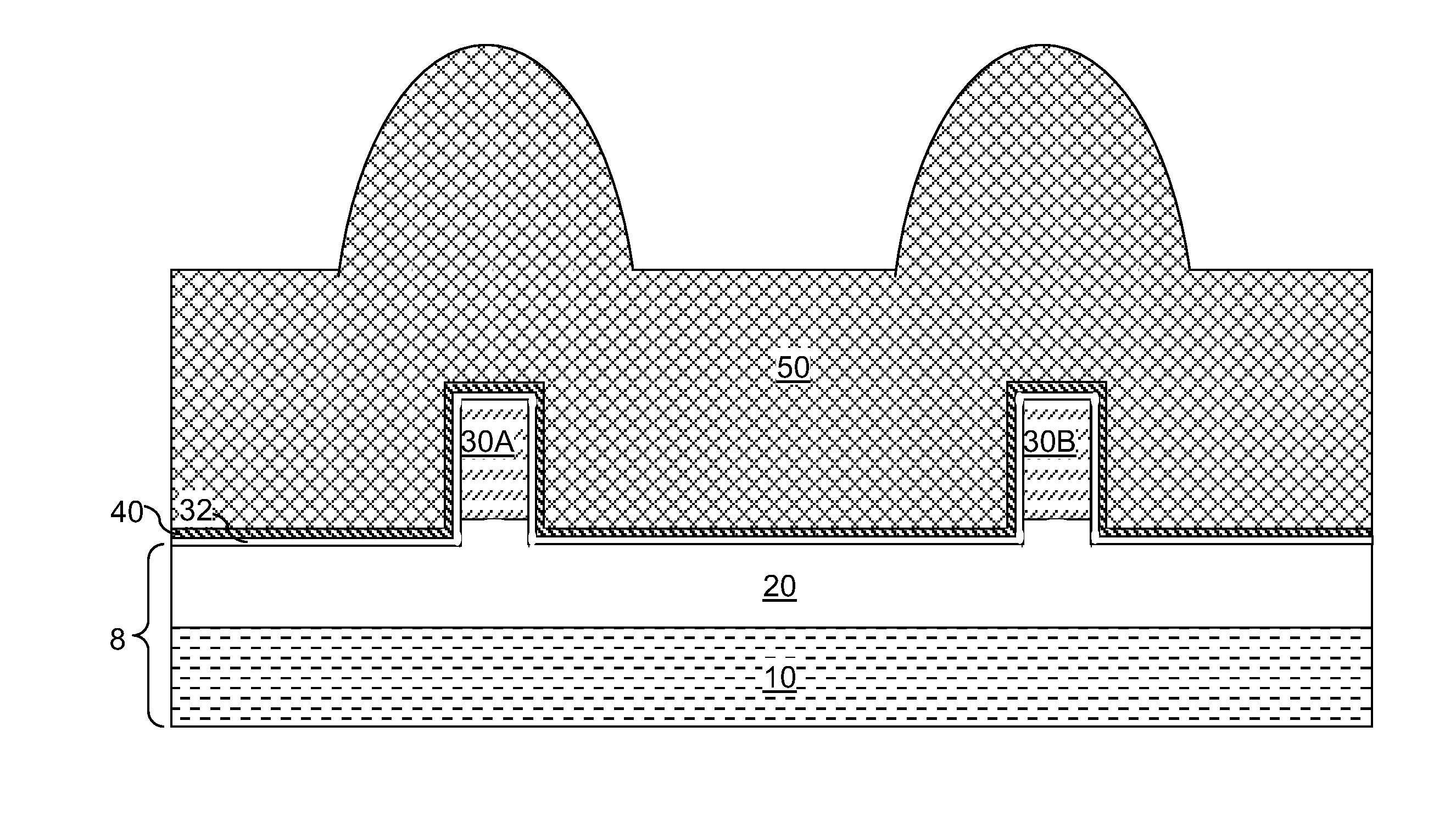
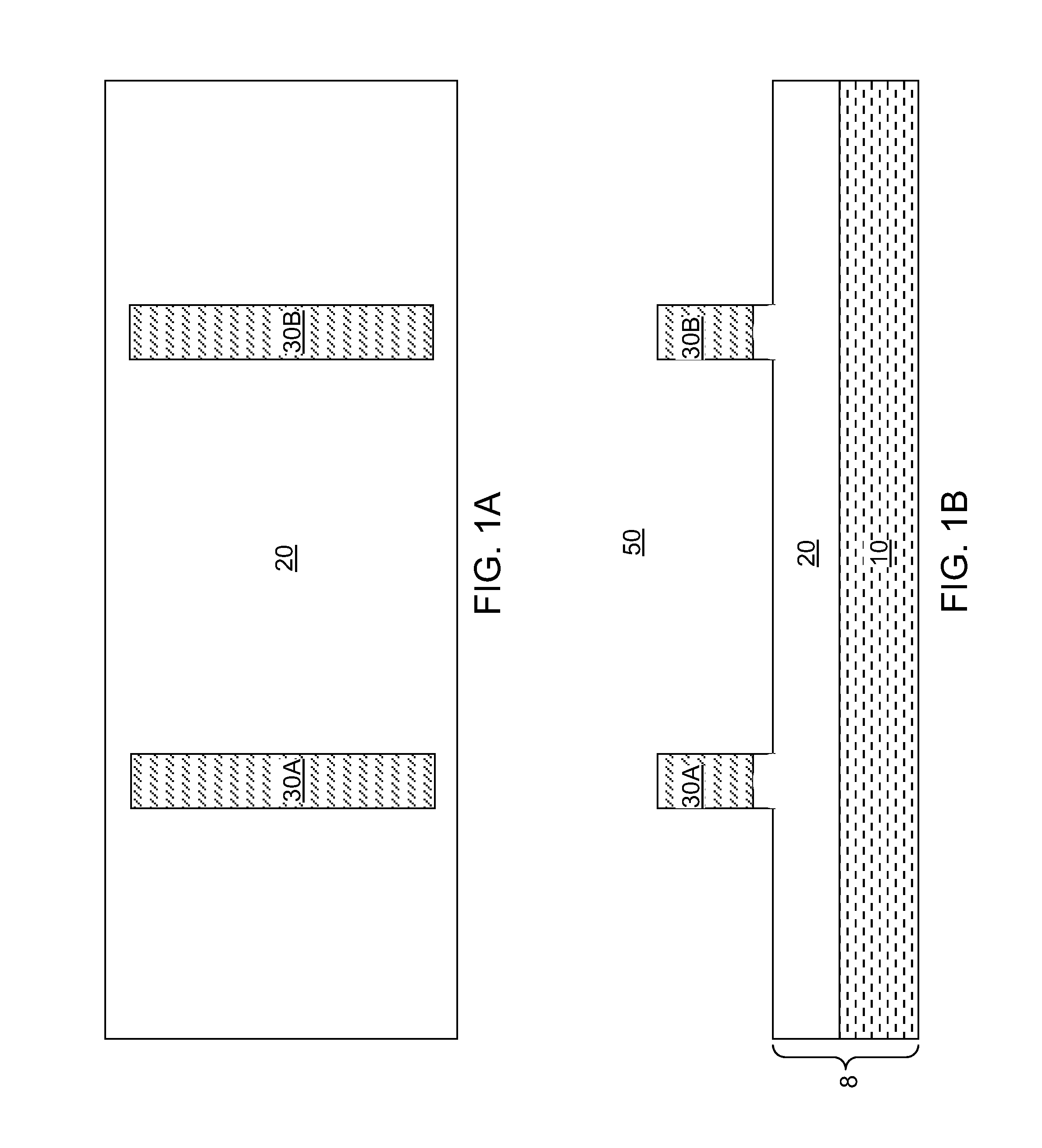
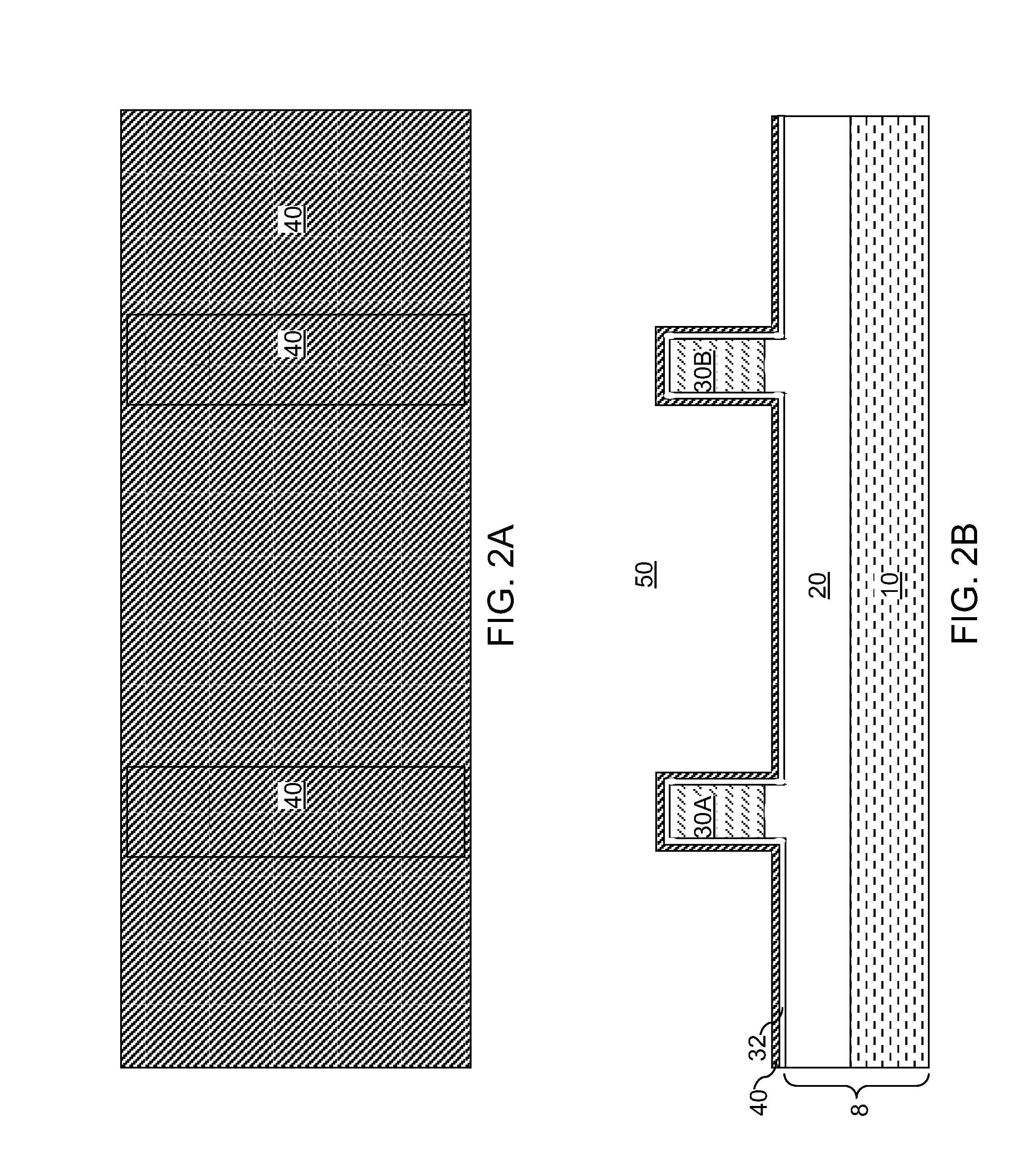
[0041]Referring to FIGS. 1A and 1B, a first exemplary semiconductor structure according to the present disclosure includes a substrate 8 and a first semiconductor material portion 30A and a second semiconductor material portion 30B. The substrate 20 can include a stack of an insulator layer 20 and a handle substrate 10. The first semiconductor material portion 30A and the second semiconductor material portion 30B can be a pair of semiconductor fins having shapes of rectangular parallelepipeds.

[0042]In one embodiment, the first exemplary semiconductor structure can be formed by patterning a semiconductor-on-insulator (SOI) substrate that includes the handle substrate 10, the insulator layer 20 as a buried insulator layer, and a top semiconductor layer. The handle substrate 10 can include a semiconductor material, an insulator material, or a conductive material, and provides mechanical support to the buried insulator layer 20 and the top semiconductor layer 30. The insulator layer 20 ...

second embodiment

[0073]Referring to FIG. 11, a second exemplary semiconductor structure according to the present disclosure can be derived from the first exemplary semiconductor structure by forming a first plurality of semiconductor material fins, such as semiconductor fins, in a first area in which the first gate conductor layer 50 contacts the workfunction material layer 40 (See FIGS. 6A and 6B), and by forming a second plurality of semiconductor material portions, such as semiconductor fins, in a second area in which the second gate conductor layer 60 contacts the workfunction material layer 40 (See FIGS. 6A and 6B).

[0074]For example, a first semiconductor material portion 30A, a second semiconductor material portion 30B, a third semiconductor material portion 30C, and a fourth semiconductor material portion 30D are formed over an insulator layer 20 in a substrate (10, 20). A stack of the gate dielectric layer 32 and the workfunction material layer 40 is formed over the first, second, third, and...

fourth embodiment

[0086]Referring to FIG. 16, a fourth exemplary semiconductor structure according to the present disclosure can be derived from the first exemplary semiconductor structure by forming a first plurality of semiconductor material fins, such as active regions, in a first area in which the first gate conductor layer 50 contacts the workfunction material layer 40 (See FIGS. 14A and 14B), and by forming a second plurality of semiconductor material portions, such as active regions, in a second area in which the second gate conductor layer 60 contacts the workfunction material layer 40 (See FIGS. 14A and 14B).

[0087]For example, a first semiconductor material portion 130A, a second semiconductor material portion 130B, a third semiconductor material portion 130C, and a fourth semiconductor material portion 130D are formed over an insulator layer 20 in the substrate 8′. A stack of the gate dielectric layer 32 and the workfunction material layer 40 is formed over the first, second, third, and fou...


PUM

PropertyMeasurementUnit
gate lengthsaaaaaaaaaa
thicknessaaaaaaaaaa
thicknessaaaaaaaaaa

Abstract

A stack of a gate dielectric layer and a workfunction material layer are deposited over a plurality of semiconductor material portions, which can be a plurality of semiconductor fins or a plurality of active regions in a semiconductor substrate. A first gate conductor material applying a first stress is formed on a first portion of the workfunction material layer located on a first semiconductor material portion, and a second gate conductor material applying a second stress is formed on a second portion of the workfunction material layer located on a second semiconductor material portion. The first and second stresses are different in at least one of polarity and magnitude, thereby inducing different strains in the first and second portions of the workfunction material layer. The different strains cause the workfunction shift differently in the first and second portions of the workfunction material layer, thereby providing devices having multiple different workfunctions.

Description

BACKGROUND[0001]The present disclosure relates to a semiconductor structure and particularly to field effect transistors having workfunctions modulated by gate strain, and methods of manufacturing the same.[0002]Metal gate field effect transistors require work function modulation in order to tune threshold voltages. Typically, p-type field effect transistors require that the workfunction of the gate electrode be near the mid-band gap or the valence band edge of the semiconductor material of the channel, and n-type field effect transistors require that the workfunction of the gate electrode be near the mid-band gap or the conduction band edge of the semiconductor material. Further, multiple threshold voltages are employed within a set of field effect transistors to provide devices tailored for various purposes. For example, some field effect transistors may be optimized for high performance, and some other field effect transistors may be optimized for low power consumption.[0003]Work...

Claims


Application Information

Patent Timeline
Patent Type & Authority Applications(United States)
IPC IPC(8): H01L27/092H01L29/78
CPCH01L27/0922H01L27/0924H01L29/7845H01L27/092H01L21/823412H01L21/82345H01L21/823821H01L21/845H01L27/1211
Inventor BAJAJ, MOHITMURALI, KOTA V.R.M.NAYAK, RAHULNOWAK, EDWARD J.PANDEY, RAJAN K.
Owner INT BUSINESS MASCH CORP
Learn More