Methods for fabricating integrated circuits with a high-voltage mosfet

a high-voltage mosfet, integrated circuit technology, applied in the direction of basic electric elements, electrical apparatus, semiconductor devices, etc., can solve the problems of physical size, adversely affecting the prior or concurrent fabrication of other devices, and limited thickness of polysilicon layers

Active Publication Date: 2015-02-05
GLOBALFOUNDRIES SINGAPORE PTE LTD
View PDF0 Cites 6 Cited by
  • Summary
  • Abstract
  • Description
  • Claims
  • Application Information

AI Technical Summary

Problems solved by technology

Although the logic devices, memory devices, and high-voltage MOSFETs are often formed on the same chip and frequently share common materials, such devices do have fundamental structural differences, and they are often formed at different times during a particular process flow that is performed to form the completed integrated circuit device.
Thus, the process designer is often faced with the challenge of ensuring that process steps employed in the fabrication of one device do not harm other devices that are previously or concurrently fabricated.
With reduction in physical size, however, there is a greater likelihood that the processes employed in the fabrication of one device of the integrated circuit may adversely affect the prior or concurrent fabrication of other devices due to increased proximity of the devices.
Due to scale limitations, however, in integrated circuit designs where a logic device is disposed adjacent to the high-voltage MOSFET device, the thickness of the polysilicon layer is limited.
In particular, in small scale devices, the thickness of the polysilicon masking layer may be limited such that the thickness is insufficient to adequately block ion implantation into the channel region of the high-voltage MOSFET.
The presence of dopant ions in the channel may, in turn, result in degraded device performance.

Method used


Image

  • Methods for fabricating integrated circuits with a high-voltage mosfet
  • Methods for fabricating integrated circuits with a high-voltage mosfet
  • Methods for fabricating integrated circuits with a high-voltage mosfet

Examples


Embodiment Construction

[0013]The following detailed description is merely illustrative in nature and is not intended to limit the embodiments of the subject matter or the application and uses of such embodiments. Furthermore, there is no intention to be bound by any expressed or implied theory presented in the preceding technical field, background, brief summary or the following detailed description.

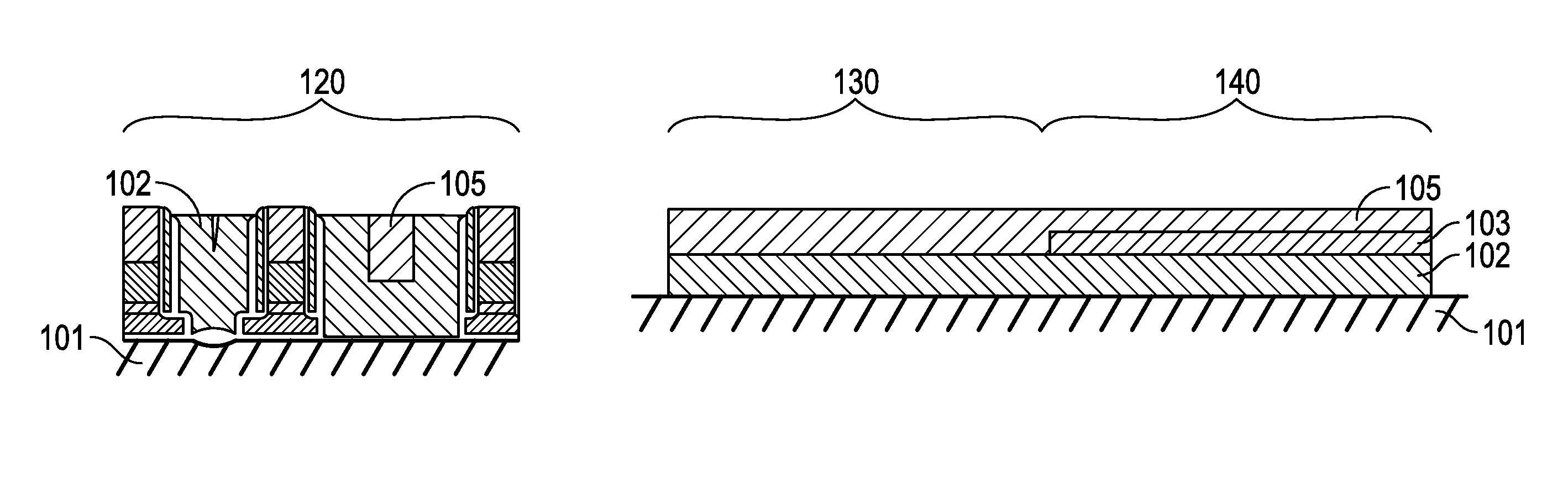
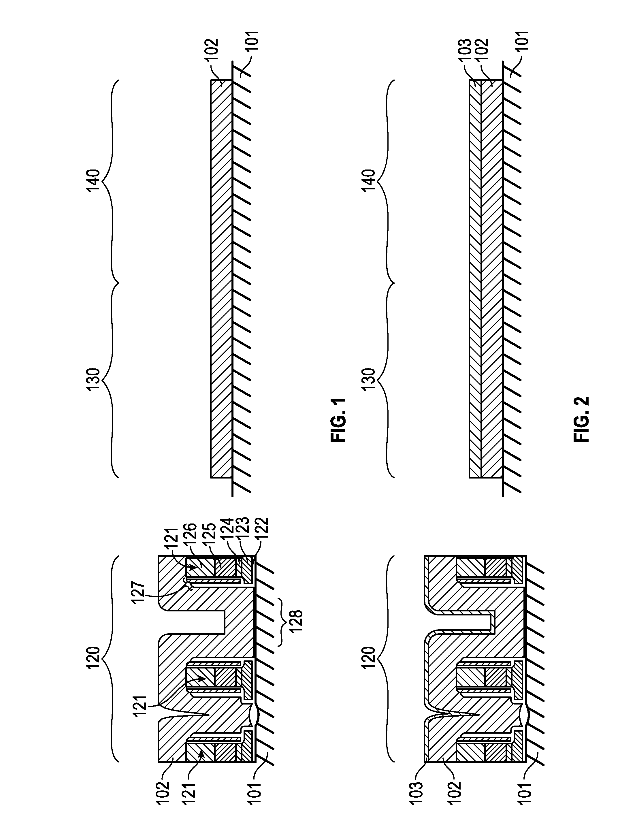
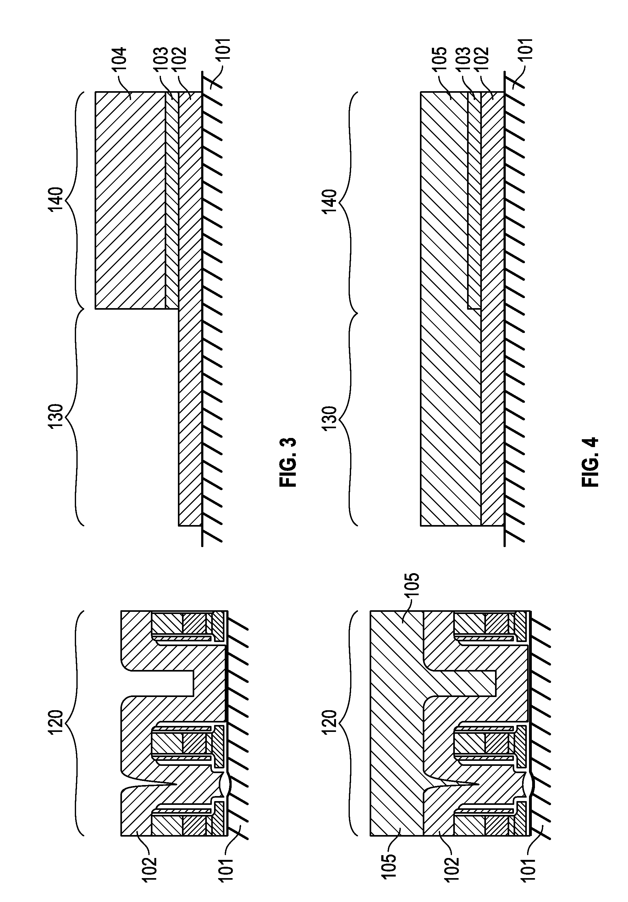
[0014]The present disclosure provides improved methods for the fabrication of integrated circuits that include high-voltage MOSFET(s), and in particular integrated circuits that include a high-voltage MOSFET, a logic device, and a memory array in close proximity to one another, such as on the same layout block of the integrated circuit. The methods described herein employ an additional “dummy” polysilicon layer or an additional “capping” silicon oxide layer that is deposited over the channel region of the high-voltage MOSFET in order to provide additional masking protection to the channel region during a subse...


PUM


Abstract

Methods for fabricating integrated circuits are disclosed. In an exemplary embodiment, a method for fabricating an integrated circuit includes forming a silicon material layer over a semiconductor substrate. The method further includes forming a capping layer over the silicon material layer and over the memory gate stack, removing the capping layer from over the memory array region and the high-voltage MOSFET region, forming a second silicon material layer over the capping layer and over the first silicon material layer, and removing the second silicon material layer. The method further includes removing the capping layer from over the first silicon material layer in the logic device region and removing the first and second silicon material layers from the high-voltage MOSFET region. Still further, the method includes forming a photoresist material layer over the memory array region and the logic device region and exposing the semiconductor substrate to an ion implantation process.

Description

TECHNICAL FIELD[0001]The present disclosure generally relates to methods for fabricating integrated circuits. More particularly, the present disclosure relates to methods for fabricating integrated circuits with a high-voltage MOSFET.BACKGROUND[0002]The majority of present day integrated circuits are implemented by using a plurality of interconnected field effect transistors (FETs), also called metal oxide semiconductor field effect transistors (MOSFETs), or simply MOS transistors. A MOS transistor includes a gate electrode as a control electrode and spaced apart source and drain regions between which a current can flow. A control voltage applied to the gate electrode controls the flow of current through a channel between the source and drain regions.[0003]The fabrication of advanced integrated circuits, such as CPUs, storage devices, ASICs (application specific integrated circuits), and the like requires the formation of a large number of circuit elements in a given chip area accor...

Claims


Application Information

Patent Timeline
Patent Type & Authority Applications(United States)
IPC IPC(8): H01L29/66
CPCH01L29/66825H01L29/7881H01L21/823418H10B41/49H10B41/43H01L29/66492
Inventor LI, BINGJUNG, SUNG MUNLIM, YI TAT
Owner GLOBALFOUNDRIES SINGAPORE PTE LTD
Why Eureka
Try Eureka