Supercharge Your Innovation With Domain-Expert AI Agents!

Memory device structure with page buffers in a page-buffer level separate from the array level

a memory device and page buffer technology, applied in semiconductor devices, digital storage, instruments, etc., can solve the problem of reducing the available area of memory cells for a given die siz

Active Publication Date: 2015-02-26
MACRONIX INT CO LTD
View PDF1 Cites 15 Cited by
  • Summary
  • Abstract
  • Description
  • Claims
  • Application Information

AI Technical Summary

Benefits of technology

The patent describes a new technology and its benefits. The patent discusses various aspects of the technology and how it can be used in different applications. By reviewing the drawings, details, and claims, it is easy to understand the technical effects of this technology.

Problems solved by technology

However, such memory device structure requires a larger area for the page buffers and reduces the available area for memory cells for a given die size.

Method used


Image

  • Memory device structure with page buffers in a page-buffer level separate from the array level
  • Memory device structure with page buffers in a page-buffer level separate from the array level
  • Memory device structure with page buffers in a page-buffer level separate from the array level

Examples


Embodiment Construction

[0022]A detailed description of embodiments of the present technology is provided with reference to the Figures.

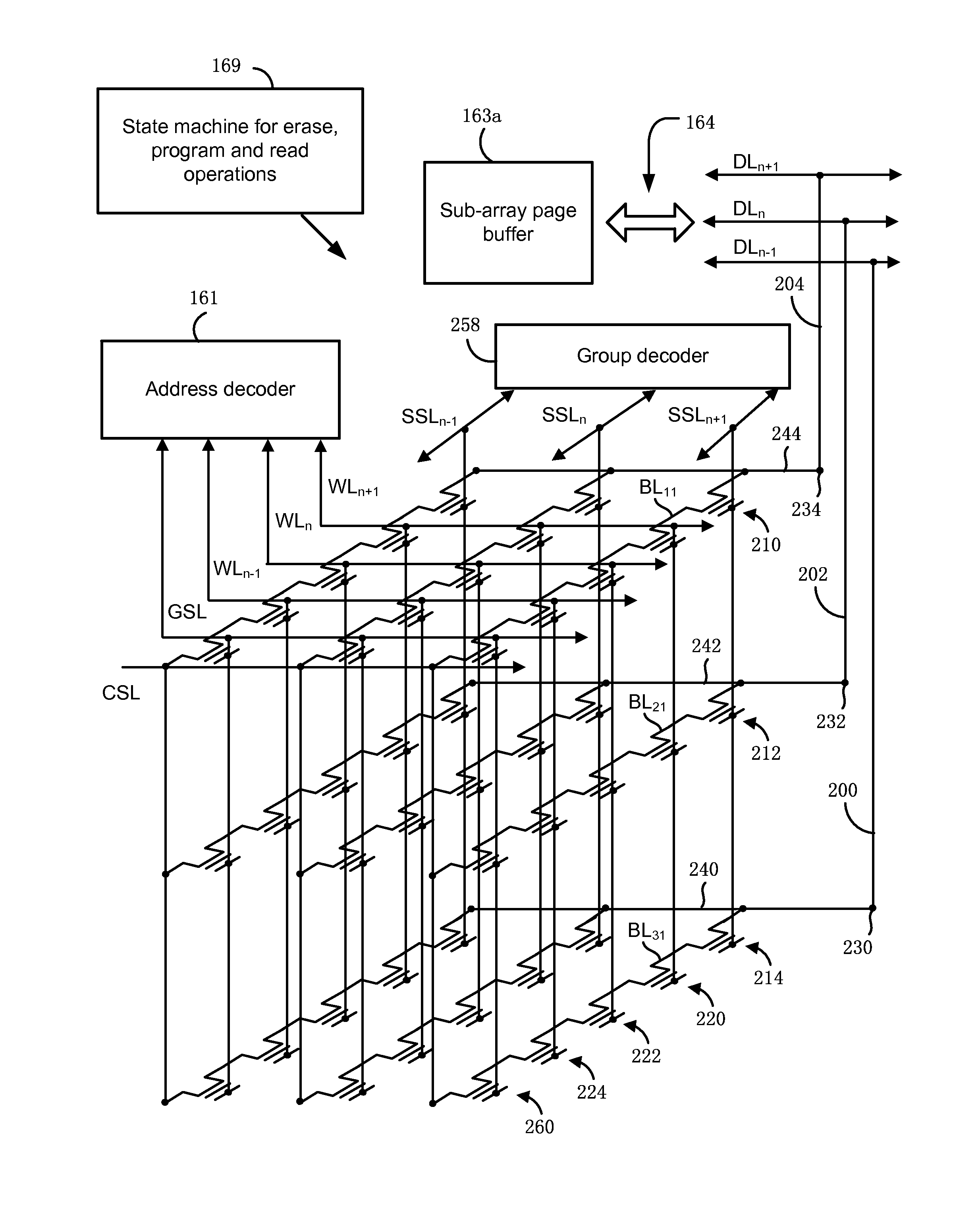
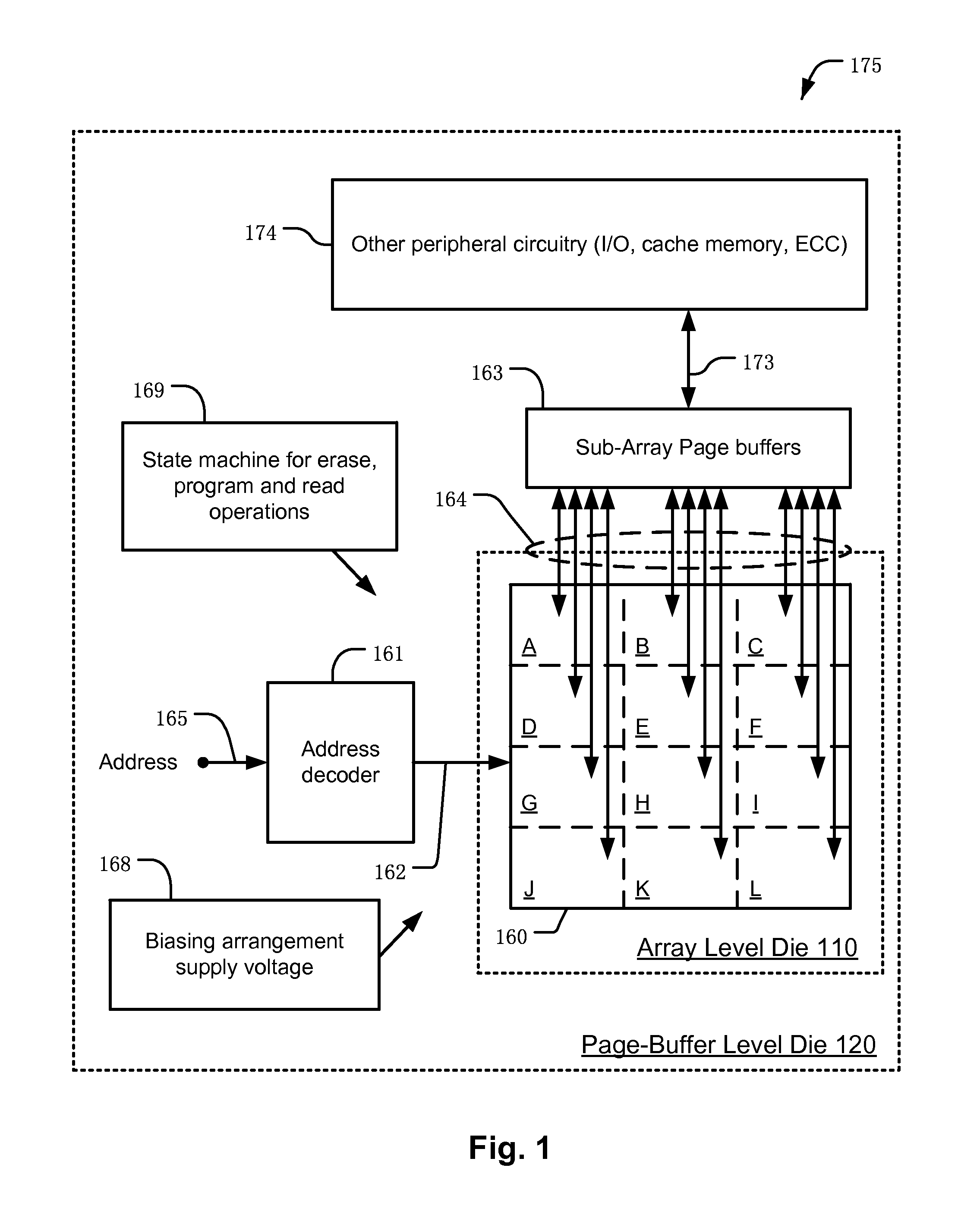
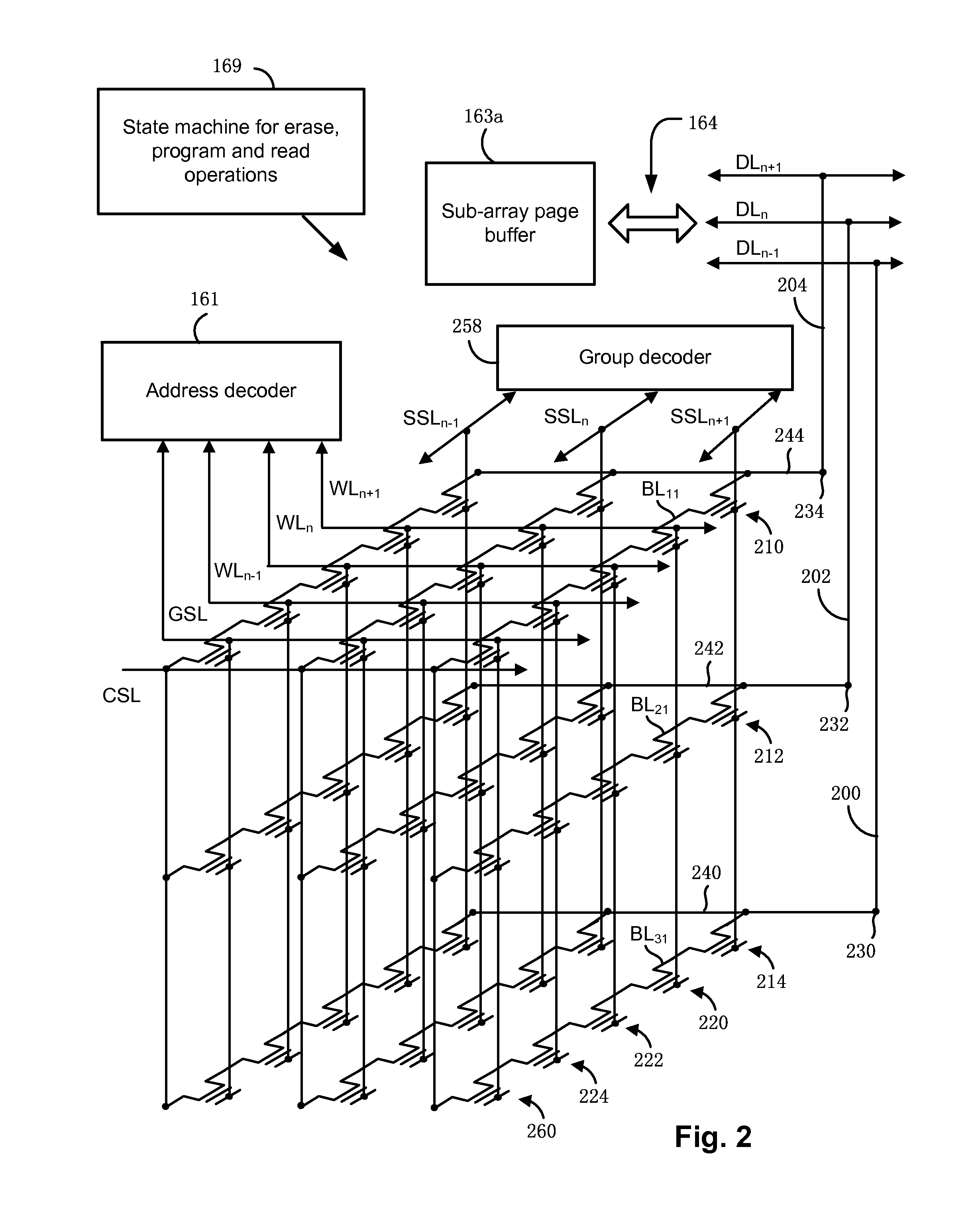
[0023]FIG. 1 is a simplified block diagram of an example memory 175 including a 3D NAND flash memory array 160 on an array die 110, and peripheral circuitry including sub-array page buffers 163 on a page-buffer level die 120. The array 160 includes a plurality of sub-arrays (A-L) of memory cells. Each sub-array can include multiple 3D memory cell blocks. Each 3D block includes multiple levels of memory cells. In the illustration, the array level die 110 is illustrated schematically as part of a flat block diagram. However, embodiments of the technology described in more detail below arrange the array level die 110 and the page-buffer level die 120 in a stacked configuration.

[0024]An address decoder 161 on the page-buffer level die 120 is coupled to the array 160 via lines 162. Addresses are supplied on bus 165 to the address decoder 161. The address decoder 161 can include...


PUM


Abstract

A structure of a memory device and a method for making the memory device structure are described. The memory device includes an array of memory cells in an array level die. The array comprises a plurality of sub-arrays. Each of the sub-arrays comprises respective data lines. The memory device also includes page buffers for corresponding sub-arrays in a page-buffer level die. The memory device also includes inter-die connections that are configured to electrically couple the page buffers in the page-buffer level die to data lines of corresponding sub-arrays in the array level die.

Description

TECHNICAL FIELD[0001]This disclosure generally relates to memory devices.DESCRIPTION OF RELATED ART[0002]Memory devices such as NAND flash memory devices utilize memory cells arranged in an array to store data. Operations can be performed on specific memory cells in the array of memory cells through the use of an address decoder that selects specific word lines and bit lines in the array. Data in the memory cells in the array can be accessed through input-output circuits and a page buffer coupled to bit lines in the array. In typical memory device structures, the address decoder is disposed adjacent to one side of the array of memory cells. The page buffer is disposed adjacent to another side of the array of memory cells. Other peripheral circuits such as input-output circuits are disposed in peripheral regions around the address decoder, the page buffer, and the array of memory cells. To provide high data rate, a large number of bit lines in parallel are disposed on top of the arra...

Claims


Application Information

Patent Timeline
Patent Type & Authority Applications(United States)
IPC IPC(8): G11C16/04G11C16/10H01L27/115H10B69/00
CPCG11C16/0483G11C16/10H01L27/11578G11C16/06G11C5/063G11C7/1006G11C11/4097G11C2207/005G11C2207/2245G11C2029/0411G11C16/16H10B43/20
Inventor CHEN, SHIH-HUNG
Owner MACRONIX INT CO LTD
Features
  • R&D
  • Intellectual Property
  • Life Sciences
  • Materials
  • Tech Scout
  • Unparalleled Data Quality
  • Higher Quality Content
  • 60% Fewer Hallucinations
Learn More